


Quick Research
Generate reliable direction feasibility study reports for your R&D in just a few steps.

Technical Q&A
Discover and master advanced knowledge NOW. Basics, ideas, possibilities, all at once.

Find Solutions
As an expert in R&D theories, this can generate solutions to your technical problems instantly.

Evaluate Feasibility
Analyze your overall solution with one click, know your potential R&D risks in advance.

Monitor Landscape
Get weekly tech updates, stay abreast of the latest tech innovations and key insights.
Grating type surface incidence type optical detector
A photodetector and grating technology, applied in the field of optical communication, can solve the problems of waveguide photodetector limitations and achieve the effects of low dark current, polarization insensitive sensitivity, and large light receiving angle
- Summary
- Abstract
- Description
- Claims
- Application Information
AI Technical Summary
Problems solved by technology
Method used
Image

Examples
Embodiment 1
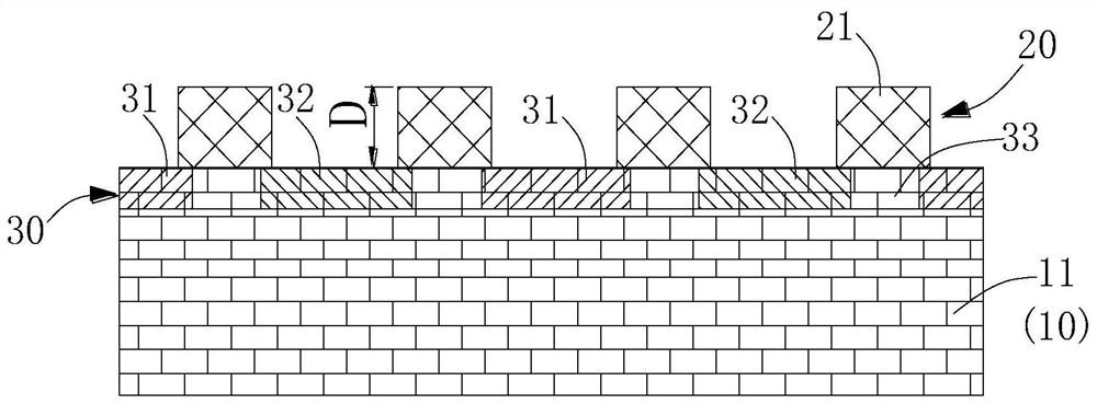
[0041] Such as figure 1 As shown, it is a schematic diagram of the chip structure of a grating-type surface-incidence photodetector according to Embodiment 1 of the present application. The detector includes a substrate 10 and a grating active layer 20 disposed on the substrate 10 . In this embodiment, the substrate 10 includes a silicon substrate 11 (ie, a silicon layer), and the grating active layer 20 includes a plurality of grating protrusions 21 . A doped layer 30 is formed on the upper surface of the silicon substrate 11, and the doped layer 30 includes a plurality of alternately arranged P-type doped electrodes 31 and N-type doped electrodes 32, and adjacent P-type doped electrodes 31 and N-type doped electrodes There is an undoped silicon region 33 between the doped electrodes 32 . The above-mentioned grating active layer 20 is disposed on the doped layer 30, and the grating protrusions 21 of the grating active layer 20 cover the undoped silicon region 33 of the doped...
Embodiment 2
[0047] The difference between this embodiment and the first embodiment is that doping is also carried out on both side walls of each grating protrusion of the grating active layer, so as to enhance the electric field intensity on the grating protrusion.
[0048] Specifically, for example, Figure 10 In the schematic diagram of the structure of the photodetector chip shown, P-type doping is performed on the side wall of the grating protrusion 21 adjacent to the P-type doped electrode 31 to form a P-type side wall 22, and the P-type side wall 22 and the P-type doped electrode 31 is conductively connected to form an electric field between the P-type doped electrode 31 and the N-type doped electrode 32 , and between the P-type sidewall 22 and the N-type doped electrode 32 to enhance the electric field intensity on the grating protrusion 21 . Alternatively, N-type doping can be carried out on the side wall of the grating protrusion adjacent to the N-type doped electrode to form an ...
Embodiment 3
[0053] Such as Figure 13 The structural diagram of the photodetector chip shown is different from the above-mentioned embodiments 1 and 2 in that the upper surface of the undoped silicon region 33 in this embodiment is lower than the P-type doped electrodes 31 and N-type doped electrodes 31 on both sides thereof. The upper surface of the impurity electrode 32 forms a groove 34 at the undoped silicon region 33 , and the bottom of each grating protrusion 21 covering the doped layer 30 covers the bottom of the corresponding groove 34 . in such as Figure 13 In the cross section shown, the cross section of the groove 34 may be a regular rectangle, or the bottom of the groove 34 may also be in other shapes such as arc or trapezoid. The depth of the groove 34 is less than the thickness of the grating active layer 20 , or less than or equal to the thickness of the doped layer 30 . This structure enables the grating active layer 20 and the doped layer 30 to have more overlapping ar...
PUM
| Property | Measurement | Unit |
|---|---|---|
| thickness | aaaaa | aaaaa |
| thickness | aaaaa | aaaaa |
| thickness | aaaaa | aaaaa |
Abstract
Description
Claims
Application Information
 - R&D Engineer
- R&D Manager
- IP Professional
- Industry Leading Data Capabilities
- Powerful AI technology
- Patent DNA Extraction
Browse by: Latest US Patents, China's latest patents, Technical Efficacy Thesaurus, Application Domain, Technology Topic, Popular Technical Reports.
© 2024 PatSnap. All rights reserved.Legal|Privacy policy|Modern Slavery Act Transparency Statement|Sitemap|About US| Contact US: help@patsnap.com