Adhesive sheet for temporary attachment and semiconductor device producing method using same
A technology for adhesives and semiconductors, applied in the direction of semiconductor devices, semiconductor/solid device manufacturing, grafted polymer adhesives, etc., can solve the problems of reduced adhesive strength, thermal decomposition, etc., to achieve reduced adhesive strength, excellent Adhesive strength, effects of excellent photoinitiation efficiency
- Summary
- Abstract
- Description
- Claims
- Application Information
AI Technical Summary
Problems solved by technology
Method used
Image
Examples
preparation example 1
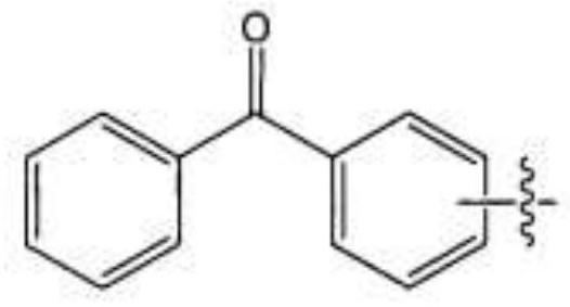
[0107] A monomer mixture consisting of 75 g of 2-ethylhexyl acrylate (2-EHA), 5 g of 4-benzoylphenyl methacrylate, and 20 g of hydroxyethyl acrylate (HEA) was placed in a reactor equipped with a cooling system to allow nitrogen reflux and easy temperature control. Subsequently, based on 100 g of the monomer mixture, 400 μm of n-DDM (n-dodecylmercaptan) as a chain transfer agent (chaintransfer agent, CTA) and 100 g of ethyl acetate (EAc) as a solvent were added thereto, and after injection Nitrogen was thoroughly mixed with each other at 30° C. for 30 minutes or longer while removing oxygen in the reactor. Then, the temperature was raised and kept at 62° C., and 300 ppm of V-60 (azobisisobutyronitrile) was added thereto as a reaction initiator to initiate a reaction, followed by polymerization for 6 hours to prepare a primary reaction material.
[0108]24g of 2-methacryloyloxyethyl isocyanate (MOI) (90mol% based on HEA in the primary reaction material) and 0.24g of catalyst (D...
preparation example 2
[0111] A monomer mixture consisting of 20 g of ethyl acrylate, 63 g of 2-ethylhexyl acrylate (2-EHA), 2 g of 4-benzoylphenyl acrylate and 15 g of hydroxyethyl acrylate (HEA) was placed in a cooling system equipped In the reactor to achieve nitrogen reflux and easy temperature control. Subsequently, based on 100 g of the monomer mixture, 400 μm of n-DDM (n-dodecylmercaptan) as a chain transfer agent (CTA) and 100 g of ethyl acetate (EAc) as a solvent were added thereto, and nitrogen gas was injected to remove The oxygen in the reactor was thoroughly mixed with each other at 30°C for 30 minutes or longer. Then, the temperature was raised and kept at 62° C., and 300 ppm of V-60 (azobisisobutyronitrile) was added thereto as a reaction initiator to initiate a reaction, followed by polymerization for 6 hours to prepare a primary reaction material.
[0112] 15 g of 2-methacryloxyethyl isocyanate (MOI) (76 mol % based on HEA in the primary reaction material) and 0.15 g of catalyst (D...
preparation example 3
[0115] With 4g TDI-based isocyanate curing agent and 3g 2,2-dimethoxy-1,2-diphenylethan-1-one as photoinitiator and 100g preparation example 1 based on (meth)acrylate The binder resin (a-1) was mixed to prepare a composition (A-3) for forming an adhesive layer.
PUM
| Property | Measurement | Unit |
|---|---|---|
| thickness | aaaaa | aaaaa |
| thickness | aaaaa | aaaaa |
| height | aaaaa | aaaaa |
Abstract
Description
Claims
Application Information
 - R&D
- Intellectual Property
- Life Sciences
- Materials
- Tech Scout
- Unparalleled Data Quality
- Higher Quality Content
- 60% Fewer Hallucinations
Browse by: Latest US Patents, China's latest patents, Technical Efficacy Thesaurus, Application Domain, Technology Topic, Popular Technical Reports.
© 2025 PatSnap. All rights reserved.Legal|Privacy policy|Modern Slavery Act Transparency Statement|Sitemap|About US| Contact US: help@patsnap.com


