Packaging structure of perovskite solar cell, and preparation method of packaging structure
A technology for solar cells and packaging structures, applied in the field of solar cells, can solve problems such as performance degradation, and achieve the effects of improving stability, low cost, and avoiding contact
- Summary
- Abstract
- Description
- Claims
- Application Information
AI Technical Summary
Problems solved by technology
Method used
Image
Examples
Embodiment 1
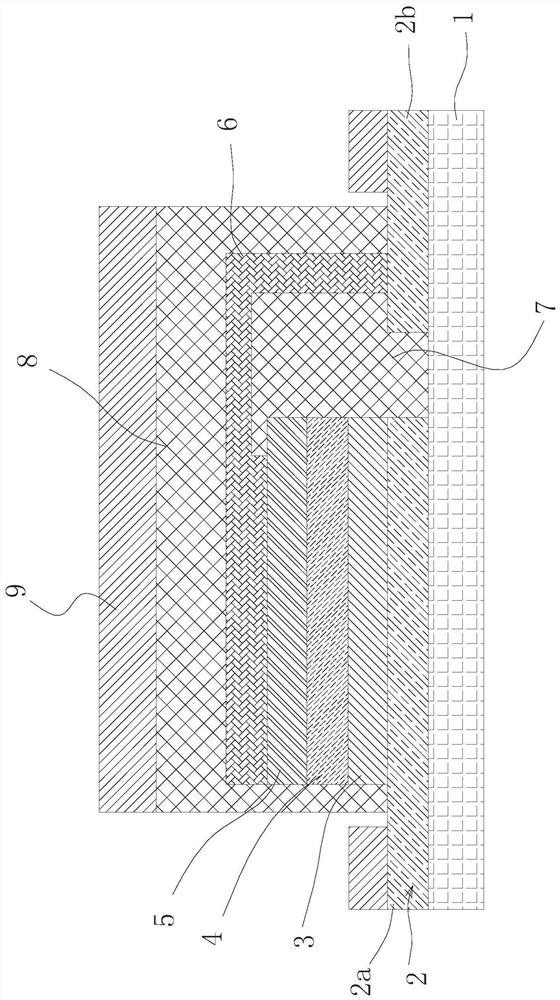
[0024] Such as figure 2 As shown, a packaging structure of a perovskite solar cell includes a substrate 1, and the substrate 1 is sequentially provided with a transparent conductive layer 2, an electron transport layer 3, a perovskite layer 4, a hole transport layer 5 and The metal electrode 6 is provided with a dense insulating layer 7 between the perovskite layer 4 and the metal electrode 6 .
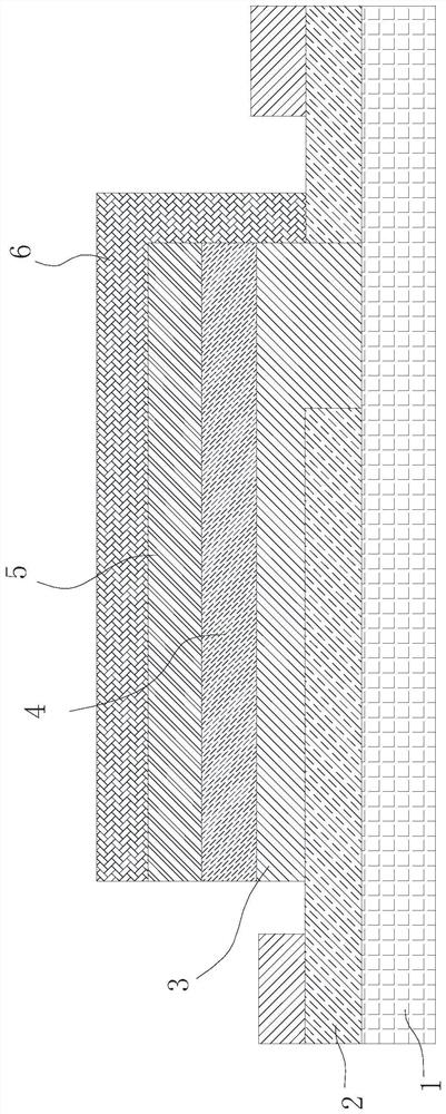
[0025] figure 1 Shown is a perovskite solar cell in the prior art. There is no dense insulating layer between the perovskite layer 4 and the metal electrode 6 . diffusion. In the present invention, a dense insulating layer 7 is provided between the perovskite layer 4 and the metal electrode 6, which cuts off the contact between the metal electrode and the perovskite layer 4, and prevents the diffusion of the metal electrode to other layers at high temperature, especially to calcium Diffusion of titanite layer 4, thus improving stability.
[0026] Specifically, the transparent con...
Embodiment 2
[0032] A method for preparing an encapsulation structure of a perovskite solar cell, combining figure 2 As shown, a transparent conductive layer 2, an electron transport layer 3, a perovskite layer 4, a hole transport layer 5, a dense insulating layer 7 and a metal electrode 6 are sequentially deposited on a substrate 1 to complete the preparation of a perovskite solar cell, and then The packaging material layer 8 and the substrate 9 are sequentially stacked on the perovskite solar cell, and the packaging is completed by a laminator. During the packaging process of the laminator, the pressing temperature is 80 to 150 degrees Celsius, and the pressing time is 1 to 60 minutes.
[0033] The substrate 1 is a glass substrate, a polyethylene terephthalate organic substrate or a polyimide organic substrate, and the transparent conductive layer 2 is FTO, ITO, AZO, GZO or Ag nanowires, prepared The method is sputtering method or sol-gel method, the thickness is 100-500nm, and the ele...
Embodiment 3
[0037] First, the glass substrate 1 is cleaned, and then the substrate 1 is covered with a mask to prepare FTO by magnetron sputtering. The background vacuum of sputtering is 5×10 -4 Pa, the sputtering power is 100W, the distance between the target and the substrate is 6cm, the working pressure is 0.8Pa, the sputtering starts after 5min of pre-sputtering, the deposition time is 5min, and the sputtering thickness is 300nm, and the transparent conductive layer 2 is deposited. Remove when ready. The mask plate separates the transparent conductive layer 2 into a first conductive portion 2 a and a second conductive portion 2 b with a gap.
[0038] Then paste the tape on some areas to prepare the mask of the electron transport layer 3, and use the tape to cover the area except the first conductive part 2a. The electron transport layer is prepared by the sol-gel method, and 2% mass fraction of SnO is prepared first. 2 The colloidal precursor solution was stirred evenly, and 60 micro...
PUM
| Property | Measurement | Unit |
|---|---|---|
| thickness | aaaaa | aaaaa |
| thickness | aaaaa | aaaaa |
| thickness | aaaaa | aaaaa |
Abstract
Description
Claims
Application Information
 - R&D Engineer
- R&D Manager
- IP Professional
- Industry Leading Data Capabilities
- Powerful AI technology
- Patent DNA Extraction
Browse by: Latest US Patents, China's latest patents, Technical Efficacy Thesaurus, Application Domain, Technology Topic, Popular Technical Reports.
© 2024 PatSnap. All rights reserved.Legal|Privacy policy|Modern Slavery Act Transparency Statement|Sitemap|About US| Contact US: help@patsnap.com


