


Quick Research
Generate reliable direction feasibility study reports for your R&D in just a few steps.

Technical Q&A
Discover and master advanced knowledge NOW. Basics, ideas, possibilities, all at once.

Find Solutions
As an expert in R&D theories, this can generate solutions to your technical problems instantly.

Evaluate Feasibility
Analyze your overall solution with one click, know your potential R&D risks in advance.

Monitor Landscape
Get weekly tech updates, stay abreast of the latest tech innovations and key insights.
LED chip pad printing device capable of customizing arrangement scheme
A technology of LED chips and pad printing devices, which is applied in the direction of electrical components, semiconductor/solid-state device manufacturing, and circuits. Low, ingenious effect of the overall structure
- Summary
- Abstract
- Description
- Claims
- Application Information
AI Technical Summary
Problems solved by technology
Method used
Image

Examples
Embodiment 1
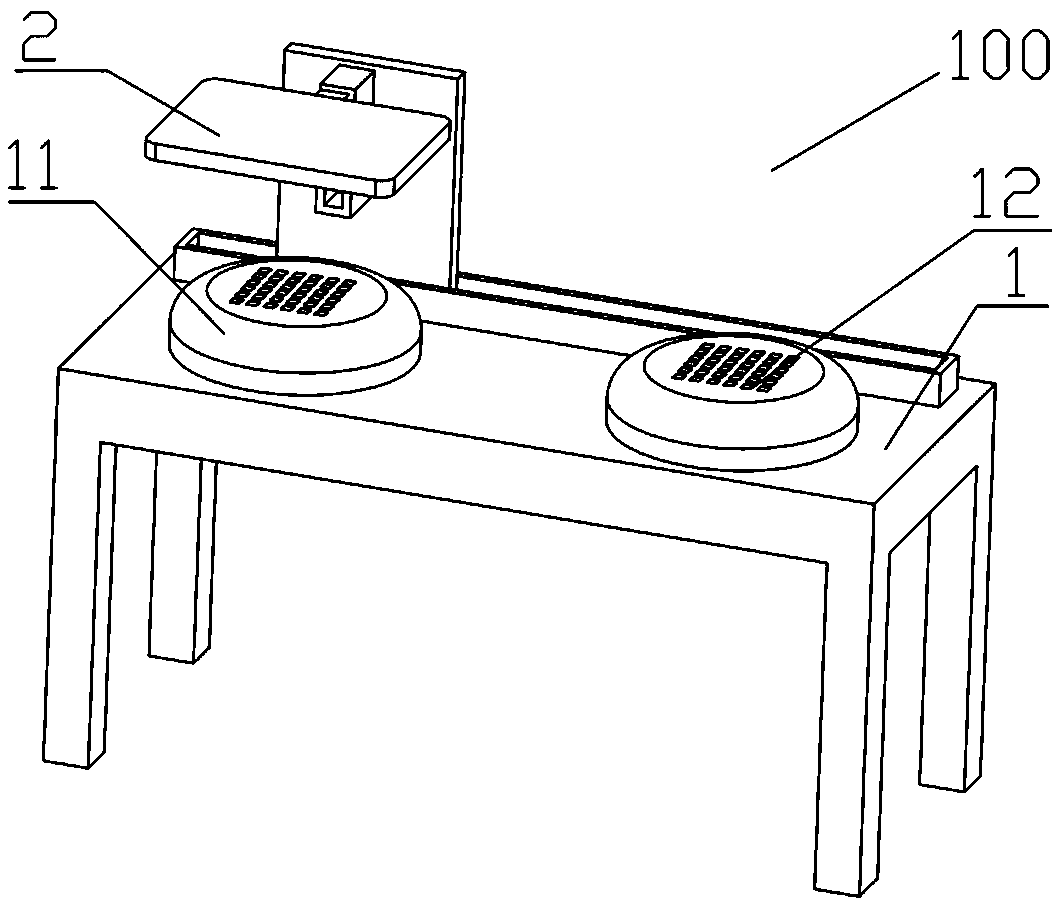
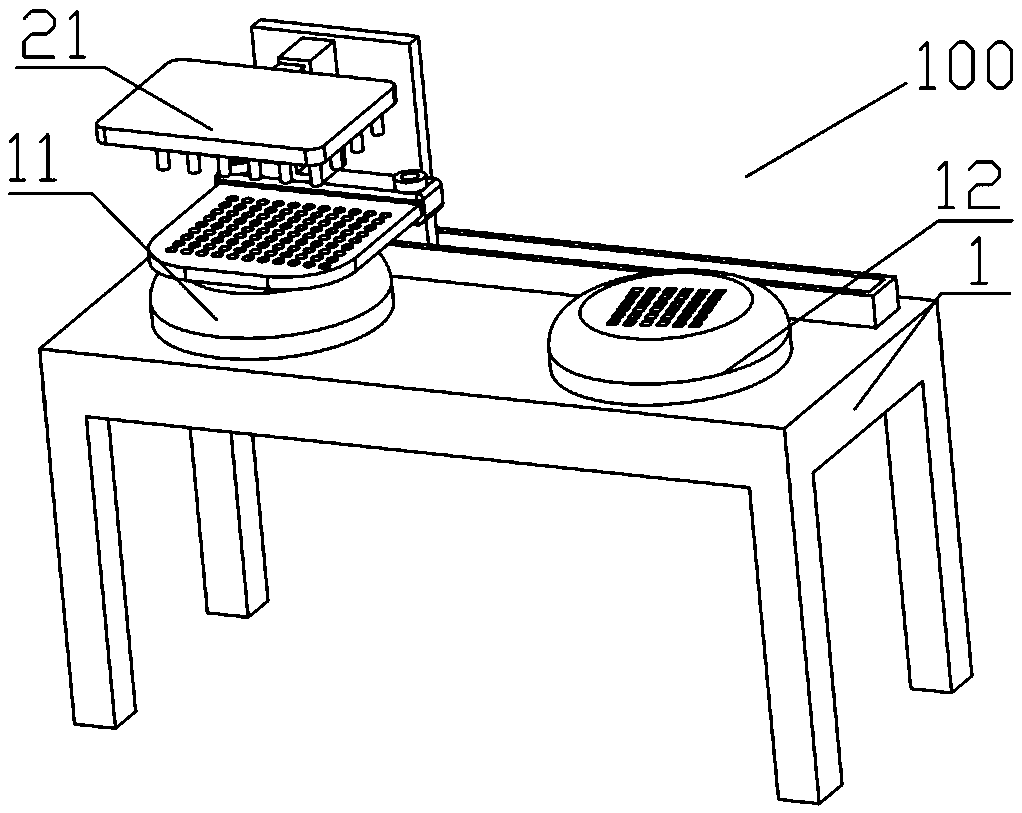
[0039] Please refer to Figure 1 to Figure 2 , an LED chip pad printing device 100 with a customizable arrangement scheme in the embodiment, including a pad printing platform 1 and an addressing adsorption control device 2; the pad printing platform 1 is provided with an initial fixed station and a target fixed station, The initial fixed station is provided with an LED chip carrier 11, and the target fixed station is provided with a target carrier 12; the addressing adsorption control device 2 includes an adsorption mechanism 21, a CCD optical positioning centering device and a wafer scanning block coordinate positioning system, the addressing adsorption control device 2 realizes transferring the LED chips on the LED chip carrier 11 to the on target vehicle 12.
[0040] The LED chip carrier 11 is customized, that is, the size and shape of the LED chip carrier 11 can be customized according to customer requirements, and can be 4 inches, 6 inches, 8 inches and other different s...
Embodiment 2
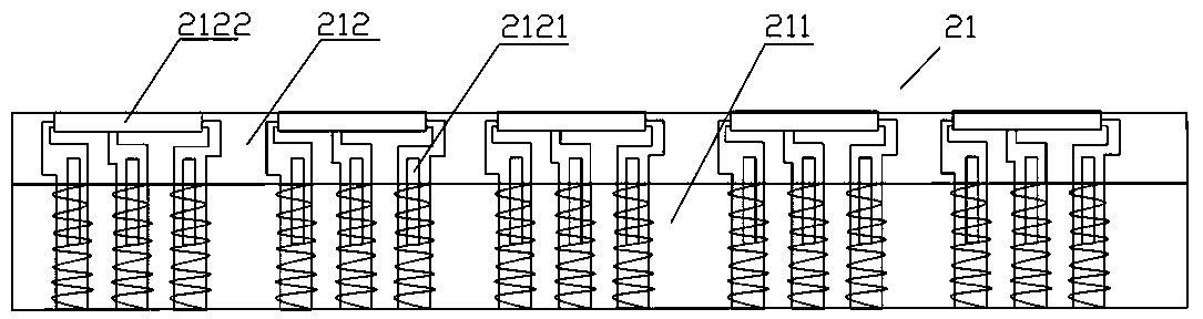
[0049] Please refer to image 3 , Figure 4 with Figure 5 The difference between embodiment 2 and embodiment 1 is that the adsorption mechanism 21 includes a magnet array template 221 and a conductive coil plate 222, and the conductive coil plate 222 is uniformly arranged with adsorption holes according to the chip unit pitch, and the adsorption Conductive coils are arranged in the holes, and the conductive coils in the adsorption holes are connected in series. The magnetic conductor array template 221 is arranged with several magnetic conductors 2121 according to the required array, and the conductive coil plate 222 can be lifted and arranged on the Above the LED chip carrier 11 and the adsorption holes correspond to the LED chips one by one, the magnetic conductor array template 221 can be lifted and arranged above the conductive coil plate 222 and the magnetic conductor 2121 and the adsorption holes corresponding settings.
[0050] Specifically, a threaded groove is pro...
Embodiment 3
[0054] Please refer to Image 6 The difference between embodiment 3 and embodiment 2 is that the adsorption mechanism 21 includes a magnet array template 221 and a conductive coil plate 222, and the conductive coil plate 222 is evenly arranged with a number of adsorption holes according to the chip unit pitch, so Conductive coils are provided on the outer wall of the conductive coil plate 222, and the magnetic conductor array template 221 is provided with a number of magnetic conductors 2121 arranged in an array as required. In addition, the suction holes correspond to the LED chips one by one, the magnetic conductor array template 221 can be lifted and lowered above the conductive coil plate 222 and the magnetic conductors 2121 are correspondingly provided to the suction holes.
[0055] Specifically, the outer side of the conductive coil plate 222 is provided with a threaded groove, and the threaded groove is used to fix and wind the conductive coil. One end of the conductive...
PUM
 Abstract
Description
Claims
Application Information
 - R&D Engineer
- R&D Manager
- IP Professional
- Industry Leading Data Capabilities
- Powerful AI technology
- Patent DNA Extraction
Browse by: Latest US Patents, China's latest patents, Technical Efficacy Thesaurus, Application Domain, Technology Topic, Popular Technical Reports.
© 2024 PatSnap. All rights reserved.Legal|Privacy policy|Modern Slavery Act Transparency Statement|Sitemap|About US| Contact US: help@patsnap.com