
Circuit structure for improving peeling strength of pins in COF-IC packaging process

A COF-IC, peel strength technology, applied in the direction of circuits, electrical components, electric solid devices, etc., can solve the problems of small adhesion strength of flexible substrates, circuit break or short circuit, copper wire stripping substrates, etc., to improve product quality efficiency, increase product life, and enhance the effect of adhesion strength

Pending Publication Date: 2020-08-04
APLUS SEMICON TECH CO LTD
View PDF0 Cites 0 Cited by
  • Summary
  • Abstract
  • Description
  • Claims
  • Application Information

AI Technical Summary

Problems solved by technology

[0004] In order to overcome the problems in the prior art that the adhesion strength of the copper wire to the flexible substrate is small, and it is easy to be affected by the subsequent processing to cause the copper wire to break or the copper wire to peel off the substrate, resulting in circuit breakage or short circuit, the present invention provides an improved Line Structure of Lead Peel Strength in COF-IC Packaging Process

Method used


Image

  • Circuit structure for improving peeling strength of pins in COF-IC packaging process
  • Circuit structure for improving peeling strength of pins in COF-IC packaging process
  • Circuit structure for improving peeling strength of pins in COF-IC packaging process

Examples


Embodiment 1

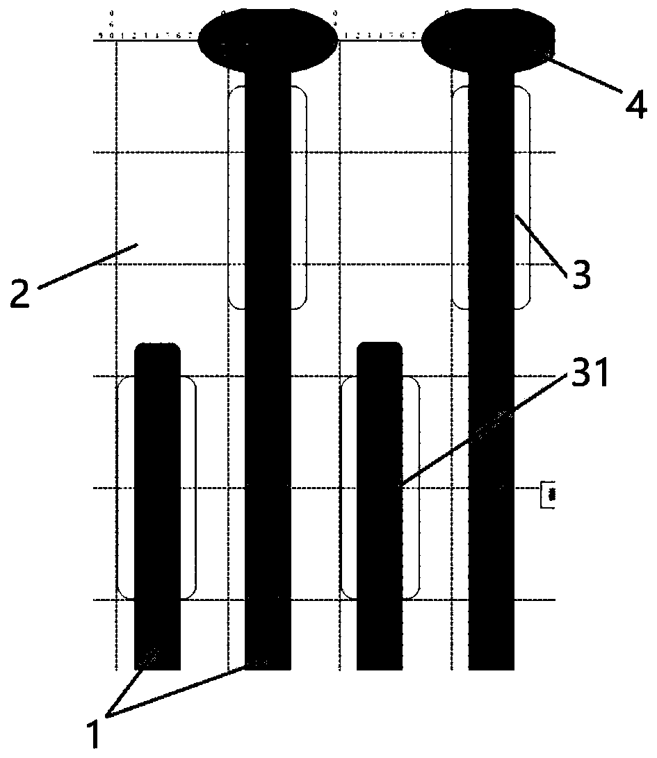
[0033] Such as figure 1 As shown, the copper wire 1 is attached to the flexible substrate 2, and the pins of the IC chip are fixedly connected to the pins of the copper wire 1 by pressure welding. The pins of the copper wire 1 are located at the end of the copper wire 1, and the copper wire 1 The pins include long pins 3 and short pins 31, the long pins 3 and short pins 31 are arranged at intervals, the long pins 3 have the same structure as the copper wire 1, and are long strips; the short pins 31 and the copper wire 1 The structures are the same, and are in the shape of a strip; the upper end of the long pin 3 is fixed with a wire reel 4, and the wire reel 4 is elliptical.

Embodiment 2

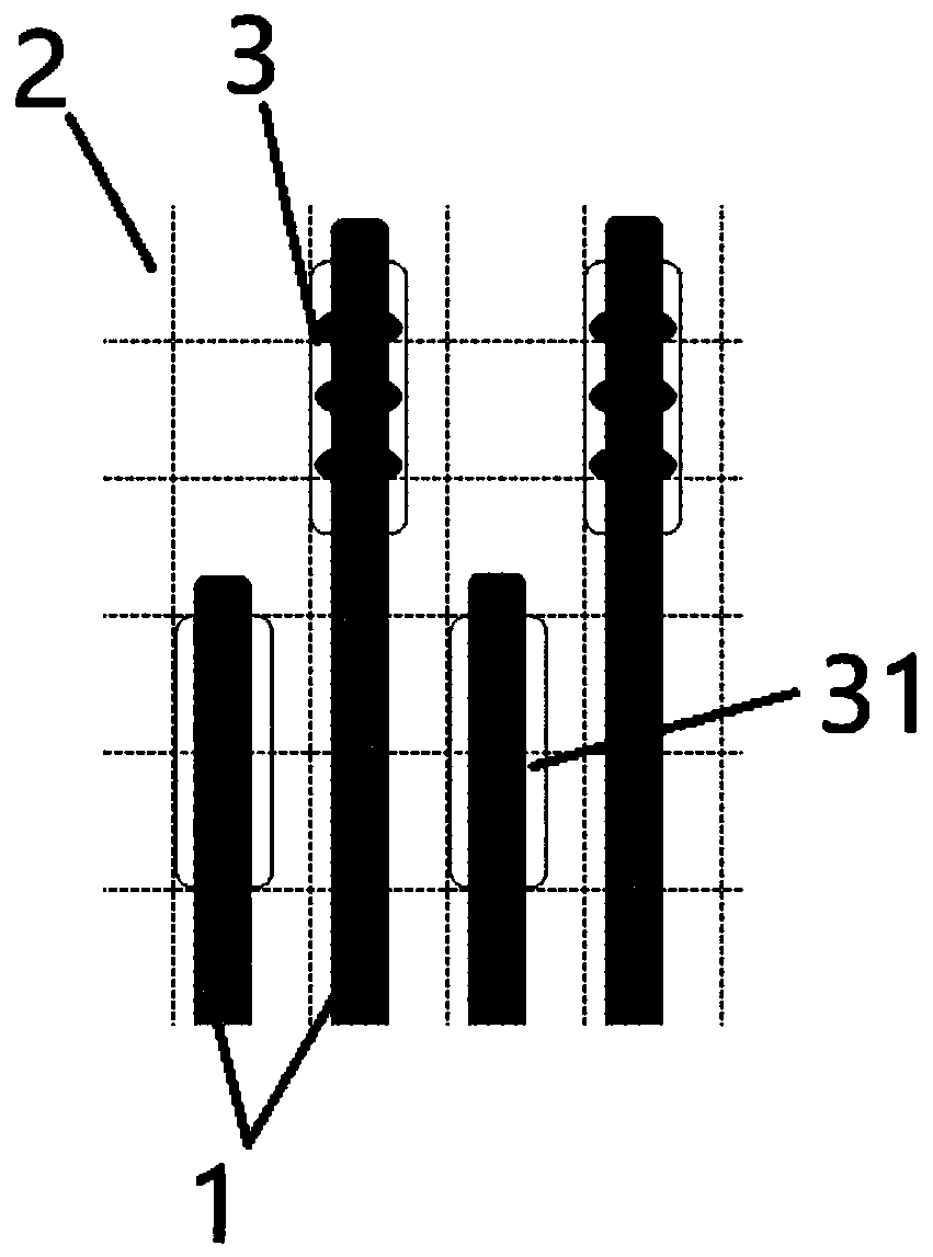
[0035] Such as figure 2 As shown, the copper wire 1 is attached to the flexible substrate 2, and the pins of the IC chip are fixedly connected to the pins of the copper wire 1 by pressure welding. The pins of the copper wire 1 are located at the end of the copper wire 1, and the copper wire 1 The pins include long pins 3 and short pins 31, and the long pins 3 and short pins 31 are arranged at intervals; the short pins 31 have the same structure as the copper wire 1, and are long strips; the long pins 3 are two-sided The extended "Feng"-shaped structure has an oval-shaped extension.

Embodiment 3

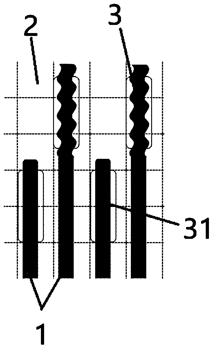
[0037] Such as image 3 As shown, the main structure of embodiment 3 is the same as that of embodiment 2, the difference is that the long pin 3 is a wave-shaped structure.


PUM


Abstract

The invention provides a circuit structure for improving the peeling strength of pins in a COF-IC packaging process. The circuit structure comprises copper wires, a flexible base material and an IC chip, the copper wires are attached to the flexible base material, pins of the IC chip are fixedly connected with pins of the copper wires in a pressure welding mode, the pins of the copper wires are located at the ends of the copper wire, the pins of the copper wires comprise long pins and short pins, the long pins and the short pins are arranged at intervals, and the circuit shapes and structuresof the long pins and the short pins are different from those of the copper wires. According to the invention, the pins of the IC chip and the pins of the copper wires are crimped; by changing the edgeshape of the joint of the pin of the copper wire and the flexible base material, the problems of plastic deformation of a single combination area of the pin of the copper wire and the flexible base material due to external load, temperature stress and residual stress, and excessive concentration of stress generated by a crack source and non-uniform structure are solved.

Description

technical field [0001] The invention relates to the technical field of chip-on-chip films, in particular to the technical field of circuit structures for improving pin peeling strength in the COF-IC packaging process. Background technique [0002] COF-IC packaging refers to the use of internal pin welding equipment to press-weld the ultra-fine line on the carrier tape and the pins of the display driver chip under specific conditions to achieve COF-IC packaging. [0003] During processing, on the one hand, because the line width of the ultra-fine line is less than 10 microns, the contact area between the line and the flexible substrate is limited, and the line width cannot be adjusted due to the influence of space; The joint strength with the chip pins is limited; it is also affected by the side erosion phenomenon in the process of circuit processing. The end of the copper wire welding area is often irregular or the side erosion is serious, which will damage the adhesion of t...

Claims


Application Information

Patent Timeline
IPC IPC(8): H01L23/49
CPCH01L23/49
Inventor 蔡水河
Owner APLUS SEMICON TECH CO LTD
Learn More