A kind of preparation method of tungsten disulfide single crystal with controllable number of layers
A tungsten disulfide single crystal and single crystal technology, applied in chemical instruments and methods, single crystal growth, single crystal growth, etc., can solve the problems of unsteady control, poor experimental repeatability, and inaccurate control, etc., and achieve the preparation repetition rate High effect of high utilization rate of raw materials
- Summary
- Abstract
- Description
- Claims
- Application Information
AI Technical Summary
Problems solved by technology
Method used
Image
Examples
Embodiment 1
[0055] Example 1 WS 2 Preparation of sample α
[0056] (1) Micropatterned WO 3 Precursor preparation:
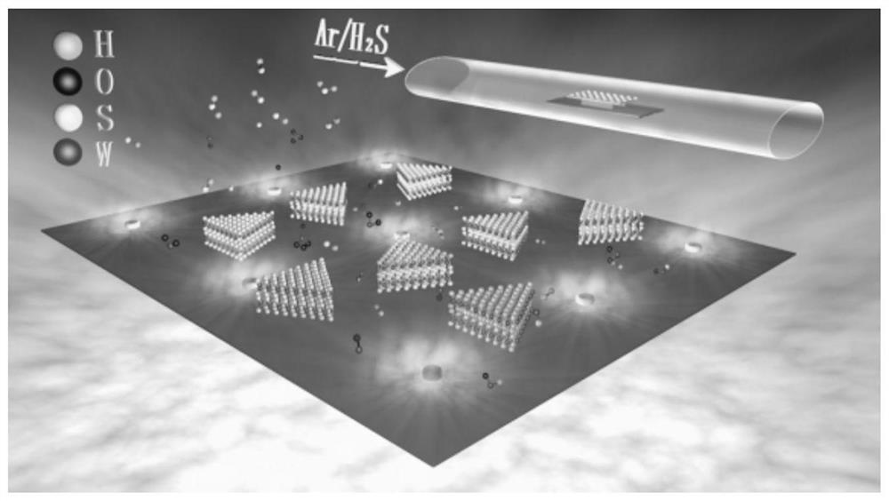
[0057] Place the hollow plate (the hollow pattern on the plate is a circular array) on 285nm SiO 2 / Si substrate (that is, the surface layer is 285nmSiO 2 silicon wafer), placed together in the coating machine, by thermal evaporation on 285nm SiO 2 Micropatterned WO with a thickness of 3 nm evaporated on Si substrate 3 source (or WO 3 precursor): at 285nm SiO 2 / Si substrate, WO 3 The diameter of the circular array is 150 μm, and the distance between the center of the circle is 450 μm, such as figure 1 shown.
[0058] (2) Preparation of WS by chemical vapor deposition (CVD) 2 :
[0059] (2.1) Micropatterned WO plated with a thickness of 3nm 3 source of SiO 2 / Si substrate is placed in the center of the heating zone of the tube furnace, and 300 sccm argon gas is introduced into the tube furnace for 30 minutes to exhaust the air in the tube furnace;
[0060] (2.2...
Embodiment 2
[0061] Example 2 WS 2 Preparation of sample β
[0062] (1) Micropatterned WO 3 Precursor preparation:
[0063] Place the hollow plate (the hollow pattern on the plate is a circular array) on 285nm SiO 2 / Si substrate (that is, the surface layer is 285nmSiO 2 silicon wafer), placed together in the coating machine, by thermal evaporation on 285nm SiO 2 Micropatterned WO with a thickness of 3 nm evaporated on Si substrate 3 source (or WO 3 precursor): at 285nm SiO 2 / Si substrate, WO 3 The diameter of the circular array is 150 μm, and the distance between the centers of the circles is 450 μm.
[0064] (2) Preparation of WS by chemical vapor deposition (CVD) 2 :
[0065] (2.1) Micropatterned WO plated with a thickness of 3nm 3 source of SiO 2 / Si substrate is placed in the center of the heating zone of the tube furnace, and 300 sccm argon gas is introduced into the tube furnace for 30 minutes to exhaust the air in the tube furnace;
[0066] (2.2) Adjust the argon flow...
Embodiment 3
[0067] Example 3 WS 2 Preparation of sample γ
[0068] (1) Micropatterned WO 3 Precursor preparation:
[0069] Place the hollow plate (the hollow pattern on the plate is a circular array) on 285nm SiO 2 / Si substrate (that is, the surface layer is 285nmSiO 2 silicon wafer), placed together in the coating machine, by thermal evaporation on 285nm SiO 2 Micropatterned WO with a thickness of 3 nm evaporated on Si substrate 3 source (or WO 3 precursor): at 285nm SiO 2 / Si substrate, WO 3 The diameter of the circular array is 150 μm, and the distance between the centers of the circles is 450 μm.
[0070] (2) Preparation of WS by chemical vapor deposition (CVD) 2 :
[0071] (2.1) Micropatterned WO plated with a thickness of 3nm 3 source of SiO 2 / Si substrate is placed in the center of the heating zone of the tube furnace, and 300 sccm argon gas is introduced into the tube furnace for 30 minutes to exhaust the air in the tube furnace;
[0072] (2.2) Adjust the argon gas ...
PUM
 Abstract
Description
Claims
Application Information
 - R&D
- Intellectual Property
- Life Sciences
- Materials
- Tech Scout
- Unparalleled Data Quality
- Higher Quality Content
- 60% Fewer Hallucinations
Browse by: Latest US Patents, China's latest patents, Technical Efficacy Thesaurus, Application Domain, Technology Topic, Popular Technical Reports.
© 2025 PatSnap. All rights reserved.Legal|Privacy policy|Modern Slavery Act Transparency Statement|Sitemap|About US| Contact US: help@patsnap.com


