Preparation method of gallium nitride molybdenum disulfide mixed-scale pn junction

A gallium nitride and molybdenum sulfide technology, which is applied in semiconductor/solid-state device manufacturing, electrical components, circuits, etc., can solve the problems of unsatisfactory test requirements and low yield, and achieve simple operation, small damage, and obvious rectification effect of effect

Active Publication Date: 2021-11-23
NJU OPTOELECTRONICS ENG RES INST CO LTD
View PDF0 Cites 0 Cited by
  • Summary
  • Abstract
  • Description
  • Claims
  • Application Information

AI Technical Summary

Problems solved by technology

The first one is to prepare n-MoS on p-GaN by traditional mechanical exfoliation method 2 , the device size is usually less than ten microns, and the yield is low
The second is to grow n-MoS directly on p-GaN by CVD synthesis 2 Films, whose size is mostly around one micron, cannot meet the requirements of the test

Method used


Image

  • Preparation method of gallium nitride molybdenum disulfide mixed-scale pn junction
  • Preparation method of gallium nitride molybdenum disulfide mixed-scale pn junction
  • Preparation method of gallium nitride molybdenum disulfide mixed-scale pn junction

Examples


Embodiment 1

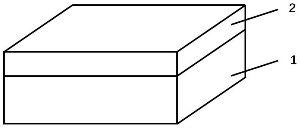
[0026] (1) PA-MBE method deposits 400-500nm p-GaN on sapphire substrate, growth method: metal gallium and nitrogen are used as Ga source and N source respectively, and the growth temperature is 890°C; N 2 The flow rate is 0.7sccm, the power is 450W; the Ga source temperature is 1050°C, and metal magnesium is used as the Mg source, and its temperature is 240°C. When the temperature rises to the desired temperature, first open the Ga baffle to grow a fresh GaN layer on the substrate surface for 2 minutes, then open the Mg baffle to start growth, and the growth time is 2 hours;

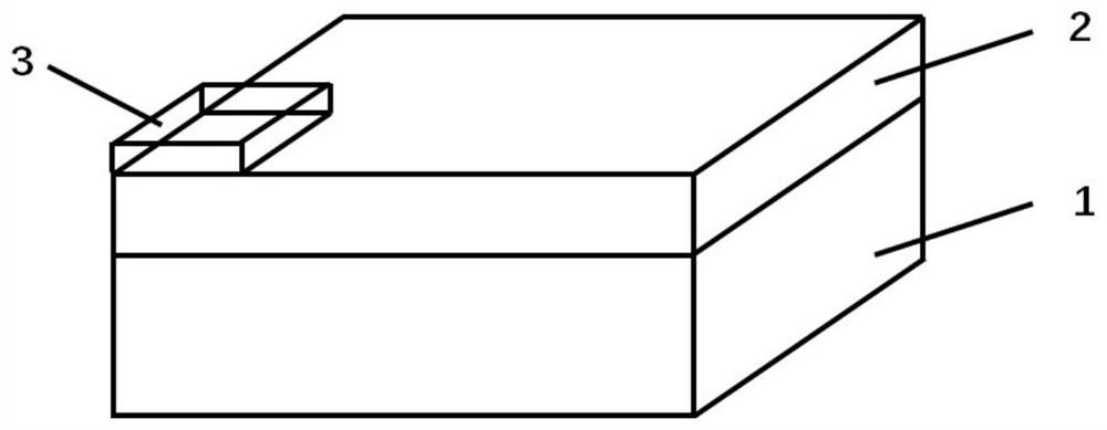
[0027] (2) Prepare Ti / Al / Ni / Au alloy electrodes on p-GaN by physical vapor deposition, the thickness of which is 30nm / 150nm / 50nm / 100nm, and then perform rapid annealing treatment on the sample in an annealing furnace under the condition of 800 °C, N 2 atmosphere, forming an ohmic contact with p-GaN;

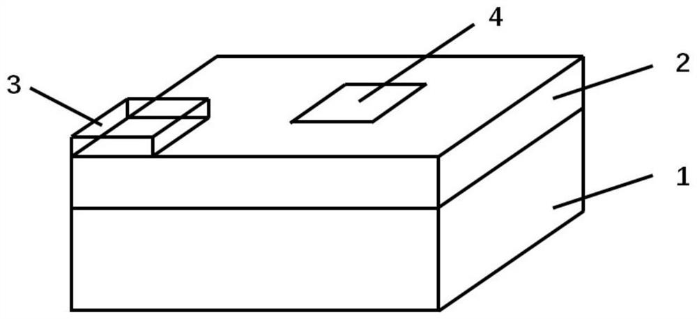
[0028] (3) Place PDMS (polydimethylsiloxane, model PF-40 / 17-X4, produced by Gel Pak Company of the Uni...


PUM

PropertyMeasurementUnit
thicknessaaaaaaaaaa
thicknessaaaaaaaaaa

Abstract

The present invention discloses a preparation method for nitride mixing melty -molybdenum -mo -molybdenum -mo -molybdenum -moralians. The steps include: (1) to deposit the P‑gan layer on the substrate;, Put a layer of uniform MOS on the surface of the tape 2 Sheet -shaped crystal, MOS is sticky with tape 2 The side of the sheet crystal is exposed to PDMS and pressed to make MOS 2 Moved to PDMS to form MOS 2 Film, remove the tape, and then buckle the Pögan layer of the device (1) device (1) to the PDMS and press it to make the MOS 2 The membrane is transferred to the surface of the P gan layer to make a mixed -scale PN knot of nitride molten molybdenum sulfide.The invention uses the PDMS auxiliary drying method to transfer, the operation is simple, and the production cost is low.MOS prepared by this method 2 The film size is large, and compared with the traditional mechanical stripping method, the sample substrate prepared by this method is relatively clean, which is convenient for subsequent device tests.

Description

technical field [0001] The invention relates to a method for preparing a gallium nitride molybdenum disulfide mixed-scale PN junction, belonging to the field of micro-nano electronic devices. Background technique [0002] Currently, the two-dimensional PN semiconductor heterojunction has become the research focus of basic science and applied physics. It can achieve new functions by combining the advantages of different materials, or regulate the properties of materials through efficient charge transport at the heterojunction interface. Photoelectric properties. Therefore, two-dimensional PN semiconductor heterojunctions have great prospects in practical applications in the fields of microelectronics and optoelectronics, such as photovoltaic devices, light emitters, and field-effect transistors. The built-in electric field and interlayer recombination existing in the PN junction will determine the rectification characteristics, photovoltaic effect and light detection ability...

Claims


Application Information

Patent Timeline
Patent Type & Authority Patents(China)
IPC IPC(8): H01L21/34
CPCH01L21/34
Inventor 曹玉洁陈敦军谢自力
Owner NJU OPTOELECTRONICS ENG RES INST CO LTD
Why Eureka
Try Eureka