Super-junction structure and manufacturing method thereof
A manufacturing method and technology of superjunction structure, applied in semiconductor/solid-state device manufacturing, semiconductor devices, electrical components, etc.
- Summary
- Abstract
- Description
- Claims
- Application Information
AI Technical Summary
Problems solved by technology
Method used
Image
Examples
no. 1 example
[0064] The super junction structure of the first embodiment of the present invention:
[0065] like Figure 1C Shown is the device structure diagram of the super junction structure of the first embodiment of the present invention; figure 2 It is a device structure diagram of a super-junction device formed by adopting the super-junction structure of the first embodiment of the present invention. The super-junction structure of the first embodiment of the present invention includes:
[0066]The first N-type sub-epitaxial layer 2 is formed in the first N-type sub-epitaxial layer 2 with first P-type sub-columns 31 and first N-type sub-columns 21 alternately arranged to form a first super-junction sub-structure.
[0067] The second N-type sub-epitaxial layer is formed on the surface of the first N-type sub-epitaxial layer 2 formed with the first superjunction sub-structure, and the second N-type sub-epitaxial layer is formed in the second N-type sub-epitaxial layer. The second N...
no. 1 example
[0090] for more clarity figure 2 The super junction device of the first embodiment of the present invention is shown, and the device structure of the first embodiment of the present invention will be described below with specific parameters:
[0091] The device in the first embodiment of the present invention is a 900V N-type superjunction MOSFET. The resistivity of the semiconductor substrate 1 is 0.001 ohm·cm to 0.003 ohm·cm, and the thickness is about 725 microns.
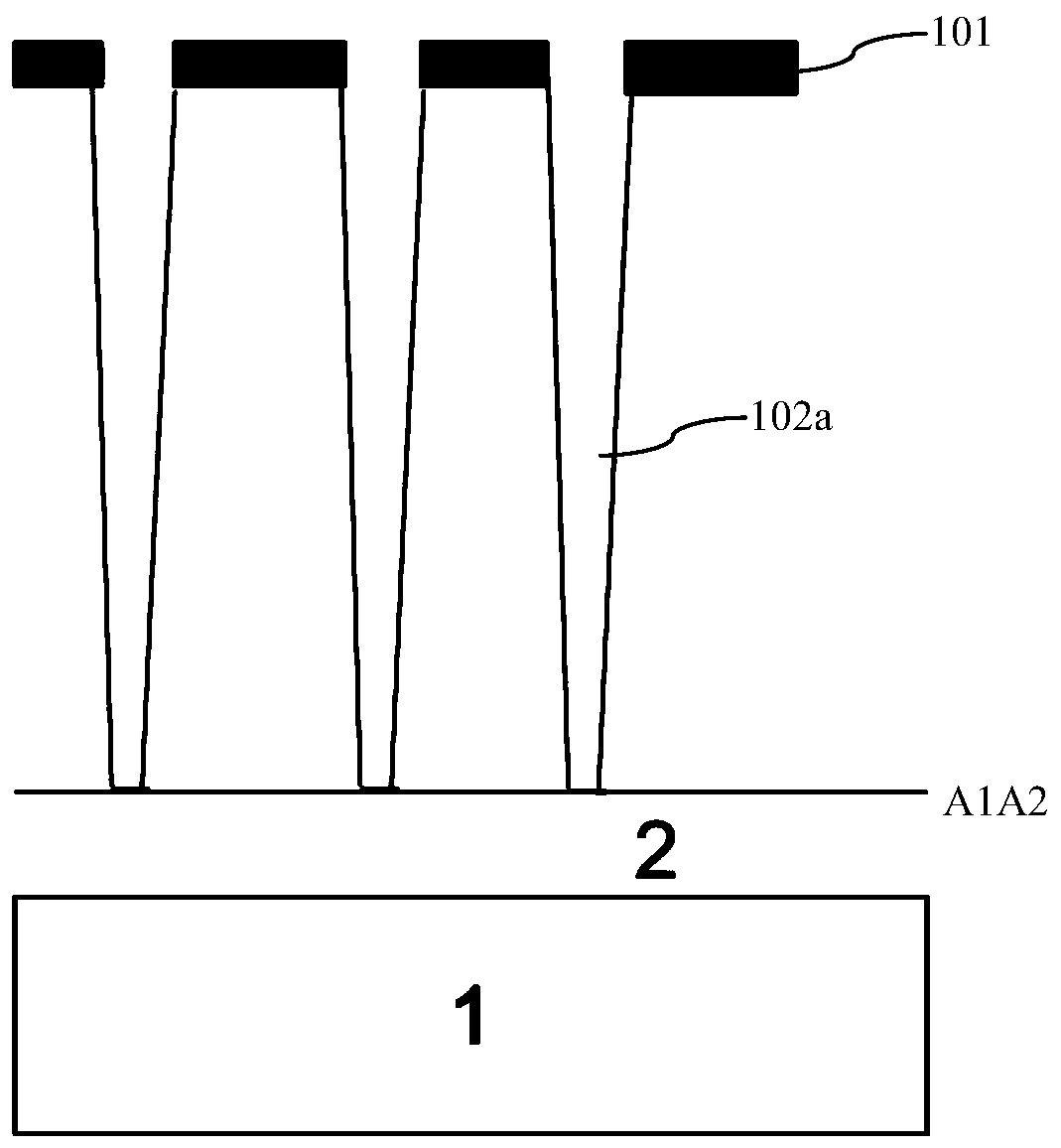
[0092] The position of the bottom surface of the first sub-trench 102a is shown by the line A1A2, and the position of the top surface of the first sub-trench 102a is shown by the line B1B2.
[0093] refer to Figure 1C As shown, the thickness of the first N-type sub-epitaxial layer 2 is 45 microns to 50 microns, the resistivity is 1.57 ohm·cm, and the doping concentration is 3.0e15cm -3 The side inclination angle of the first sub-groove 102a is 88.6 degrees, and the side inclination angle of the first sub-gro...
no. 4 example
[0119] The superjunction structure of the fourth embodiment of the present invention:
[0120] The difference between the super junction structure of the fourth embodiment of the present invention and the super junction structure of the first embodiment of the present invention is that the charge balance setting of the super junction structure of the fourth embodiment of the present invention is different, and the super junction structure of the fourth embodiment of the present invention The charge balance settings are as follows:
[0121]The side slope angle of the first sub-groove 102a is smaller than the side slope angle of the second sub-groove 102b, that is, the angle between the bottom of the first N-type sub-pillar 21 is smaller than that of the second N-type sub-pillar 22 . The bottom angle should be small. The doping concentration of the second N-type sub-column 22 is equal to the doping concentration of the first N-type sub-column 21. When the super-junction structu...
PUM
| Property | Measurement | Unit |
|---|---|---|
| Thickness | aaaaa | aaaaa |
| Thickness | aaaaa | aaaaa |
| Top width | aaaaa | aaaaa |
Abstract
Description
Claims
Application Information
 - R&D
- Intellectual Property
- Life Sciences
- Materials
- Tech Scout
- Unparalleled Data Quality
- Higher Quality Content
- 60% Fewer Hallucinations
Browse by: Latest US Patents, China's latest patents, Technical Efficacy Thesaurus, Application Domain, Technology Topic, Popular Technical Reports.
© 2025 PatSnap. All rights reserved.Legal|Privacy policy|Modern Slavery Act Transparency Statement|Sitemap|About US| Contact US: help@patsnap.com


