
Light-emitting diode based on N-type doped stack and functional layer

A technology of light-emitting diodes and doped layers, which is applied to electrical components, circuits, semiconductor devices, etc., can solve problems affecting the luminous efficiency of light-emitting diodes, and achieve the effect of improving luminous efficiency and hole concentration

Inactive Publication Date: 2020-06-23
XIAN ZHISHENG RUIXIN SEMICON TECH CO LTD
View PDF0 Cites 0 Cited by
  • Summary
  • Abstract
  • Description
  • Claims
  • Application Information

AI Technical Summary

Problems solved by technology

[0004] However, at present, because the mobility of electrons is much higher than that of holes, the number of electrons injected into the multi-quantum well light-emitting layer is too large, and it is easy to transition from the multi-quantum well light-emitting layer to the P-type semiconductor layer and undergo non-radiative recombination with holes. Affect the luminous efficiency of light-emitting diodes
And because the mobility of electrons is much higher than that of holes, the electrons generated in the N-type semiconductor layer can quickly enter the quantum well light-emitting layer, and the excess electrons will jump from the quantum well light-emitting layer to the P-type semiconductor layer, so that the electrons and Non-radiative recombination of holes affects the luminous efficiency of light-emitting diodes

Method used


Image

  • Light-emitting diode based on N-type doped stack and functional layer

Examples


Embodiment Construction

[0028] In order to make the above objects, features and advantages of the present invention more comprehensible, specific implementations of the present invention will be described in detail below in conjunction with the accompanying drawings.

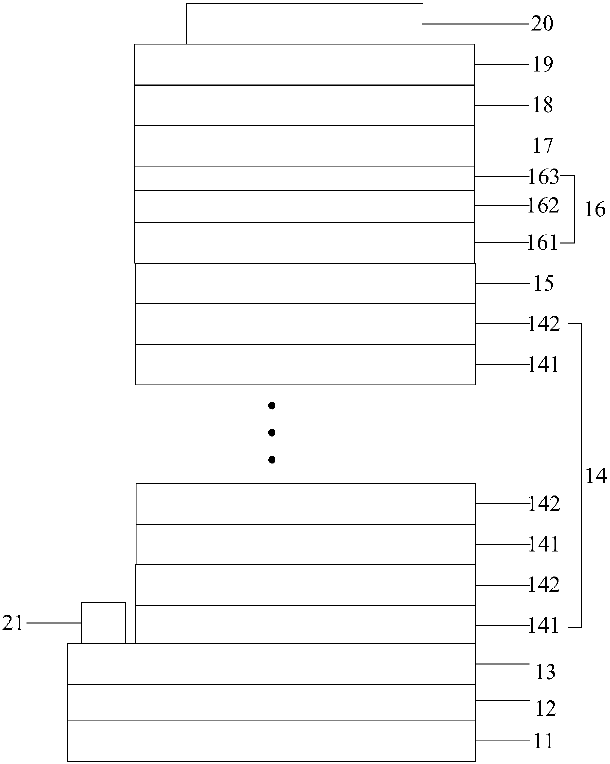
[0029] See figure 1 , figure 1 A schematic structural diagram of a light-emitting diode based on an N-type doped stack and a functional layer provided by an embodiment of the present invention. An embodiment of the present invention provides a light-emitting diode based on an N-type doped stack and a functional layer, the light-emitting diode comprising:

[0030] substrate layer 11;

[0031] Specifically, the material of the substrate layer 11 may be sapphire, silicon, silicon carbide, zinc oxide, gallium nitride, aluminum nitride or other materials suitable for crystal epitaxial growth.

[0032] The buffer layer 12 is located on the substrate layer 11;

[0033] Further, the material of the buffer layer 12 is GaN.

[0034] In the ...


PUM

PropertyMeasurementUnit
Doping concentrationaaaaaaaaaa

Abstract

The invention relates to a light-emitting diode based on an N-type doped stack and a functional layer. The light-emitting diode comprises a substrate layer, a buffer layer located on the substrate layer, an N-type semiconductor layer located on the buffer layer, an N-type doped laminated layer located on the N-type doped layer, a quantum well light-emitting layer located on the N-type doped laminated layer, a functional layer located on the quantum well light-emitting layer, a P-type doped layer located on the functional layer, and a P-type semiconductor layer located on the P-type doped layer, wherein and the N-type doped laminated layer comprises a plurality of first N-type doped layers and a plurality of second N-type doped layers; and the functional layer comprises an electron blockinglayer, a first hole injection layer and a second hole injection layer. The light-emitting diode provided by the invention is provided with the N-type doped laminated layer, so that the migration rateof electrons can be reduced, and the probability of radiative recombination between holes and electrons in the quantum well light-emitting layer can be improved by adjusting the rate of the electronsmigrated to the quantum well light-emitting layer, so that the light emitting efficiency of the light-emitting diode is improved.

Description

technical field [0001] The invention relates to the technical field of light-emitting elements, in particular to a light-emitting diode based on an N-type doped stack and a functional layer. Background technique [0002] Light Emitting Diode (LED for short) is a light emitting device that emits ultraviolet, visible or infrared light when a forward voltage is applied across a semiconductor p-n junction. It is a new generation of solid light source. Because of its small size, long life, low driving voltage, fast response, shock resistance, heat resistance and other characteristics, the efficiency of light-emitting diodes for semiconductor lighting has been continuously improved in recent years. [0003] At present, a light-emitting diode generally includes a substrate layer, a buffer layer, an N-type semiconductor layer, a multi-quantum well light-emitting layer, and a P-type semiconductor layer. Among them, the N-type semiconductor layer is used to provide electrons; the P-t...

Claims


Application Information

Patent Timeline
IPC IPC(8): H01L33/14H01L33/06
CPCH01L33/06H01L33/14H01L33/145
Inventor 李建华李全杰刘向英
Owner XIAN ZHISHENG RUIXIN SEMICON TECH CO LTD
Learn More