
Multi-stage FPGA wiring method for optimizing time division multiplexing technology

A technology of time-division multiplexing and wiring method, applied in special data processing applications, instruments, electrical digital data processing, etc., can solve the problem of increased inter-chip signal delay, and achieve optimal inter-chip signal delay and optimal inter-chip signal delay. The effect of optimizing and solving routability problems

Active Publication Date: 2020-06-19
FUZHOU UNIV
View PDF8 Cites 5 Cited by
  • Summary
  • Abstract
  • Description
  • Claims
  • Application Information

AI Technical Summary

Problems solved by technology

This can improve the routability of the entire system, but the delay of the inter-chip signal is increased

Method used

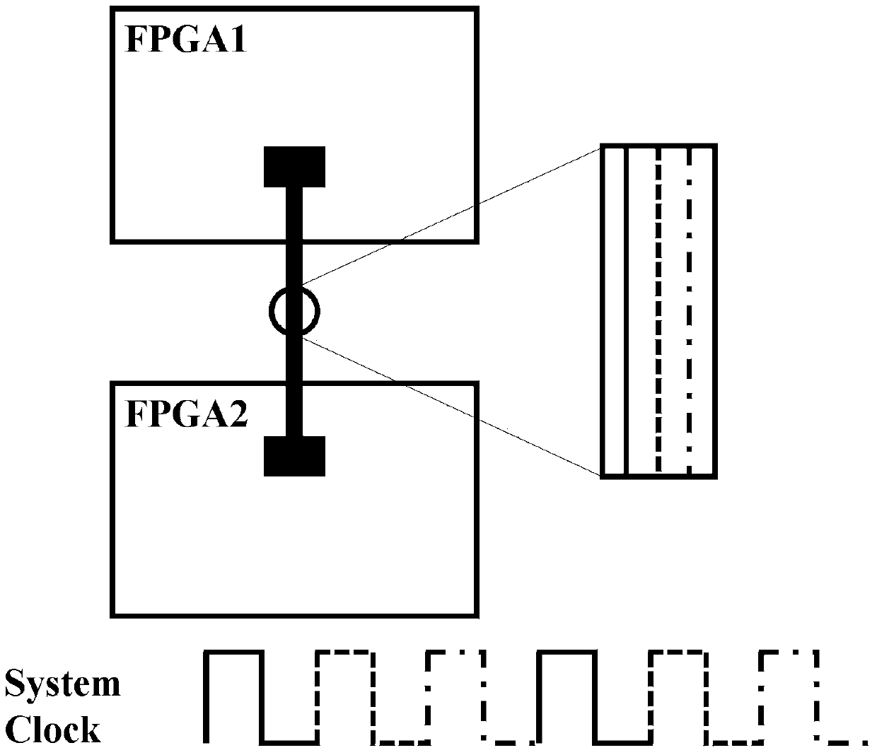
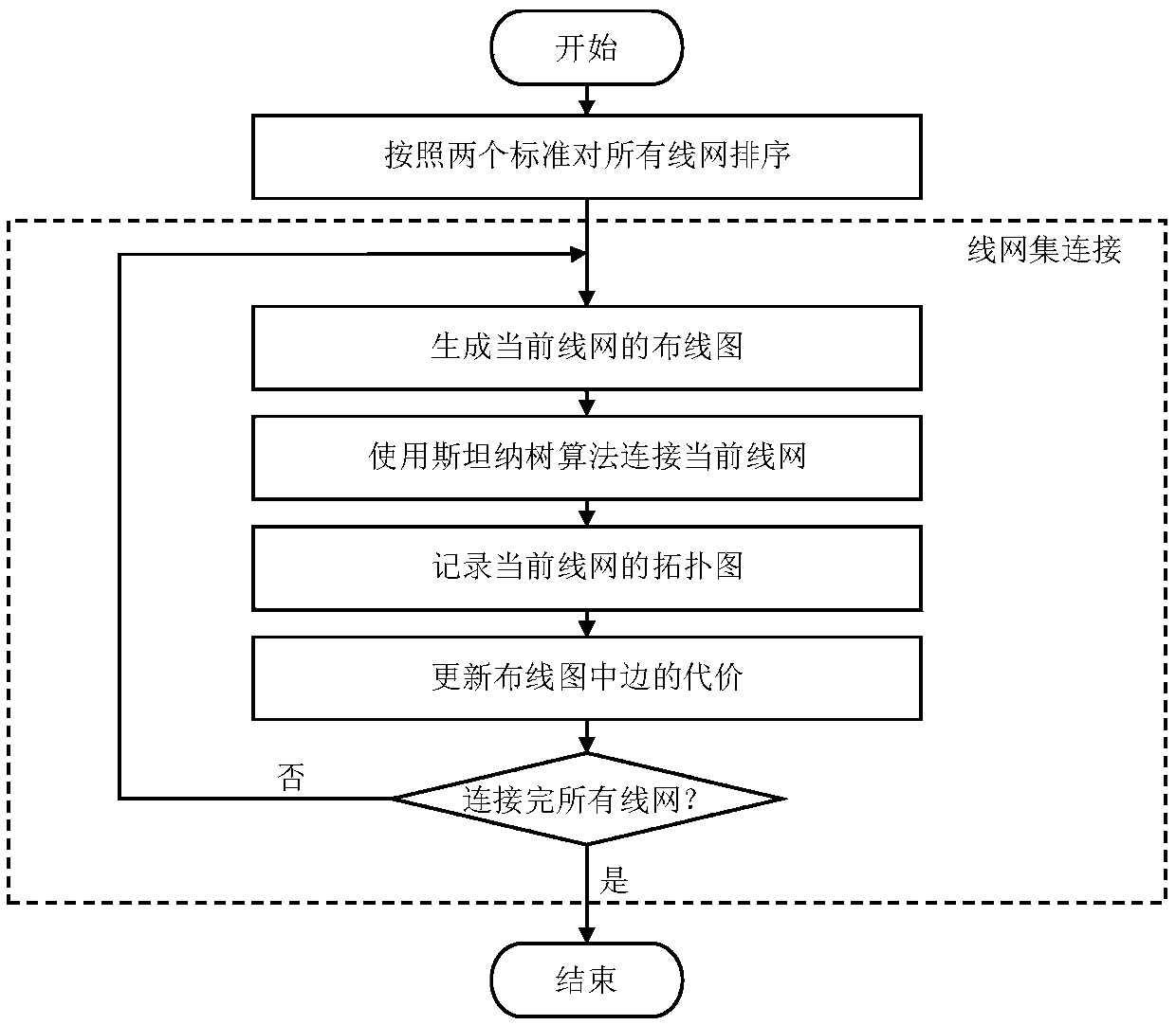

Image

  • Multi-stage FPGA wiring method for optimizing time division multiplexing technology
  • Multi-stage FPGA wiring method for optimizing time division multiplexing technology
  • Multi-stage FPGA wiring method for optimizing time division multiplexing technology

Examples


Embodiment Construction

[0064] The present invention will be further described below in conjunction with the accompanying drawings and embodiments.

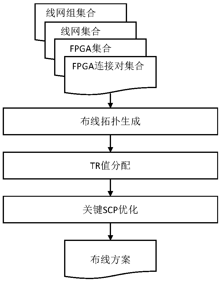
[0065] Please refer to figure 2 , the present invention provides a kind of multistage FPGA wiring method of optimization time division multiplexing technique, comprises the following steps:

[0066] Step S1: collect FPGA set, FPGA connection pair set, line net set and line net group set;

[0067] Step S2: according to the FPGA set, the FPGA connection pair set, the line net set and the line net group set, obtain the wiring topology of the line net without assigning TR;

[0068] Step S3: according to the difference of the delay situation of each wire net group, assign corresponding TR for each edge of each wire net;

[0069] Step S4: cyclically perform TR reduction and edge legalization, and iteratively optimize the net group whose TR value is greater than the preset value, until the iteration termination condition is satisfied, and an optimal wiring ...


PUM


Abstract

The invention relates to a multi-stage FPGA (Field Programmable Gate Array) wiring method for optimizing a time division multiplexing technology. The multi-stage FPGA wiring method comprises the following steps: S1, acquiring an FPGA set, an FPGA connection pair set, a wire network set and a wire network set; S2, according to the FPGA set, the FPGA connection pair set, the wire network set and thewire network set, obtaining the wiring topology of the wire network under the condition that TR is not allocated; S3, allocating a corresponding TR to each edge of each wire network according to different time delay conditions of each wire network group; and S4, circularly carrying out TR reduction and edge legalization, iteratively optimizing the wire network group of which the TR value is greater than a preset value, and obtaining an optimal wiring scheme until an iteration termination condition is met. According to the invention, the problems of inter-chip signal delay and wiring of a multi-FPGA prototype system can be optimized.

Description

technical field [0001] The invention belongs to the technical field of computer-aided design of integrated circuits, and in particular relates to a multi-stage FPGA wiring method for optimizing time-division multiplexing technology. Background technique [0002] Logic verification is an important next step in advanced nanofabrication. During the design process of a system-on-chip, it is estimated that 60% to 80% of the design time of an application-specific integrated circuit (ASIC) is spent in the verification process. Software emulation and hardware emulation are two common logic verification methods, however, software emulation needs to spend a lot of time and cost to simulate each logic gate, and the implementation cost of hardware emulation is relatively high. With the continuous development of the integrated circuit manufacturing process, the scale of the chip is getting larger and larger, and the shortcomings of the above two logic verification methods are becoming m...

Claims


Application Information

Patent Timeline
IPC IPC(8): G06F30/392G06F30/331G06N20/00
CPCG06N20/00G06F30/394G06F30/347G06F2119/12G06F30/398
Inventor 郭文忠庄震刘耿耿黄兴陈国龙
Owner FUZHOU UNIV
Learn More