


Quick Research
Generate reliable direction feasibility study reports for your R&D in just a few steps.

Technical Q&A
Discover and master advanced knowledge NOW. Basics, ideas, possibilities, all at once.

Find Solutions
As an expert in R&D theories, this can generate solutions to your technical problems instantly.

Evaluate Feasibility
Analyze your overall solution with one click, know your potential R&D risks in advance.

Monitor Landscape
Get weekly tech updates, stay abreast of the latest tech innovations and key insights.
Blind hole-filling electroplating process, plated part obtained according to process, application of plated part, and electronic product
An electroplating process and blind hole technology, applied to electrical components, circuits, printed circuits, etc., can solve problems such as long time, difficult supply of metal ions, copper thickness of copper plating surface, etc., to avoid core and missing filling, improve Distributed across the board, avoiding the effect of filling holes
- Summary
- Abstract
- Description
- Claims
- Application Information
AI Technical Summary
Problems solved by technology
Method used
Image

Examples
preparation example Construction
[0153] The preparation method of the leveling agent includes: taking 2g of N,N-dimethyl 1,4-butanediamine into a 50mL round-necked flask, then adding 5g of water into the flask, and stirring; placing the flask in an oil bath and fix it, install the condensing reflux tube on the flask; heat the oil bath to 95°C, then slowly add 2.45g of 1,7-octadiene diepoxide; Five hours; turn off the heat and continue stirring; cool to room temperature and collect the product, which is tan. Purify and dry the product to obtain a white powder, which is the leveling agent.
[0154] (c) Water washing of the test plate: two courses: the first course takes 3 minutes, and the second course takes 2 minutes.
[0155] (d) Drying of test panels.
[0156] (e) Cut the sample and make slices.
[0157] (f) Analyze slices, export data.
Embodiment 1
[0159] For blind vias with a diameter of 110 μm and a depth of 85 μm, pulse filling can effectively improve the efficiency of copper plating, which is 60% higher than that of DC electroplating.
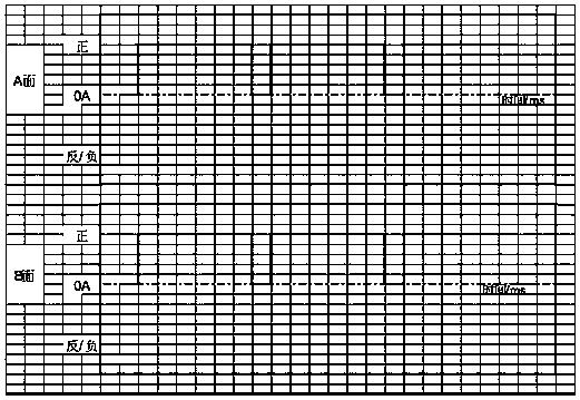
[0160] The current density was 40ASF, and the total hole-fill plating time was 35 minutes. Select positive pulse waveform: that is, forward current 40ASF, no direction current (reverse direction current is 0); forward current time is 40 milliseconds, reverse time is 0; pause time (time when current is 0) is 4 milliseconds; There is no phase difference (phase is 0), that is, the waveforms of test boards A and B are synchronized; the electroplating time is 25 minutes with waveform 1; the electroplating time is 25 minutes for waveform 2, and the electroplating is continued for 10 minutes. The combined waveforms are shown in Table 1.
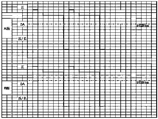
[0161] The slice picture after electroplating is as follows Figure 5 As shown, it can be seen that: 1. There is no void in the hole filling; 2. The depr...
Embodiment 2
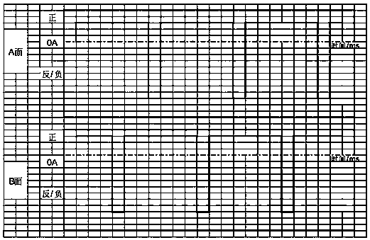
[0166] For blind holes with relatively high depth and diameter (second-order blind holes filled once), the combination of positive and negative pulse waveforms is selected, and the combined waveforms are shown in Table 2.
[0167] Table 2
[0168]
[0169] The slice picture after electroplating is as follows Figure 6 As shown, it can be seen that: 1. There is no void in the hole filling; 2. The depression is less than 10 μm; 3. The copper plating thickness is 20 μm.
[0170] Figure 6 Among them, the hole diameter is 102.07 μm, the hole depth is 122.48 μm, and the hole filling depression is 7.02 μm.
PUM
 Abstract
Description
Claims
Application Information
 - R&D Engineer
- R&D Manager
- IP Professional
- Industry Leading Data Capabilities
- Powerful AI technology
- Patent DNA Extraction
Browse by: Latest US Patents, China's latest patents, Technical Efficacy Thesaurus, Application Domain, Technology Topic, Popular Technical Reports.
© 2024 PatSnap. All rights reserved.Legal|Privacy policy|Modern Slavery Act Transparency Statement|Sitemap|About US| Contact US: help@patsnap.com