Zigzag electrode and method for improving performance of nano ultraviolet detector
A UV detector, sawtooth technology, applied in the direction of electric solid devices, circuits, electrical components, etc., can solve the problems of incompatibility between the performance of metal electrodes and process steps
- Summary
- Abstract
- Description
- Claims
- Application Information
AI Technical Summary
Problems solved by technology
Method used
Image
Examples
Embodiment approach 1
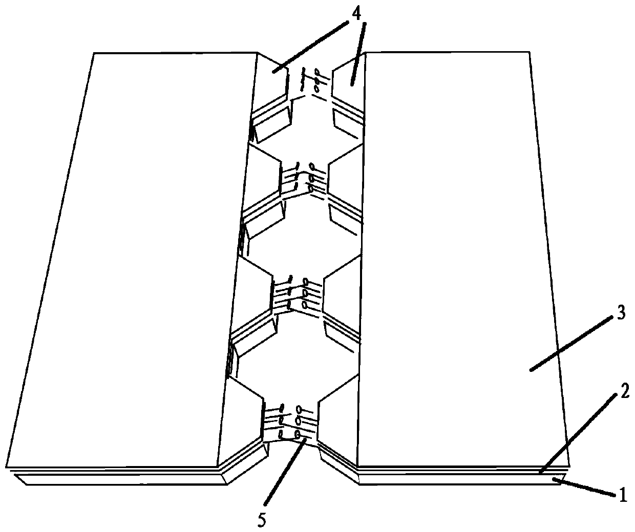
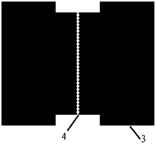
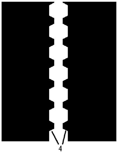
[0097] Using electron beam direct writing technology or laser direct writing technology, a lithography plate is prepared according to the layout, and the shape of the layout is the shape of a sawtooth electrode.
[0098] The surface of the silicon (Si) wafer is oxidized by a high-temperature oxidation method to form SiO with a thickness of 300 nm 2 Layer with silicon dioxide (SiO 2 ) Layer of Si as the electrode substrate, SiO 2 The layer is an insulating isolation layer.
[0099] First, use acetone to clean the electrode substrate twice, then use ethanol to clean the electrode substrate twice, and finally use deionized water to clean the electrode substrate twice. Cover the lithography plate on the cleaned electrode substrate, and use ultraviolet lithography technology to lithographically publish the picture on the electrode substrate.
[0100] Use radio frequency magnetron sputtering method to sputter a zinc oxide seed layer with a thickness of 95 nm on the lithographic layout, and...
Embodiment approach 2
[0108] Using electron beam direct writing technology or laser direct writing technology, a lithography plate is prepared according to the layout, and the shape of the layout is the shape of a sawtooth electrode.
[0109] The surface of the silicon (Si) wafer is oxidized by a high-temperature oxidation method to form SiO with a thickness of 300 nm 2 Layer with silicon dioxide (SiO 2 ) Layer of Si as the electrode substrate, SiO 2 The layer is an insulating isolation layer.
[0110] First, use acetone to clean the electrode substrate twice, then use ethanol to clean the electrode substrate twice, and finally use deionized water to clean the electrode substrate twice. Cover the lithography plate on the cleaned electrode substrate, and use ultraviolet lithography technology to lithographically publish the picture on the electrode substrate.
[0111] Use the radio frequency magnetron sputtering method to sputter a zinc oxide seed layer with a thickness of 115 nm on the lithographic layout...
PUM
| Property | Measurement | Unit |
|---|---|---|
| Length | aaaaa | aaaaa |
| Length | aaaaa | aaaaa |
| Thickness | aaaaa | aaaaa |
Abstract
Description
Claims
Application Information
 - R&D
- Intellectual Property
- Life Sciences
- Materials
- Tech Scout
- Unparalleled Data Quality
- Higher Quality Content
- 60% Fewer Hallucinations
Browse by: Latest US Patents, China's latest patents, Technical Efficacy Thesaurus, Application Domain, Technology Topic, Popular Technical Reports.
© 2025 PatSnap. All rights reserved.Legal|Privacy policy|Modern Slavery Act Transparency Statement|Sitemap|About US| Contact US: help@patsnap.com


