
Method for suppressing radio frequency loss of silicon-based gallium nitride radio frequency device

A radio frequency device, silicon-based nitrogen technology, applied in semiconductor/solid state device manufacturing, semiconductor devices, electrical components, etc., can solve the problems of increasing the conductivity of silicon substrates, large radio frequency loss of microwave radio frequency devices, etc., to reduce radio frequency loss, The effect of reducing conductivity, the method is simple, fast and effective

Pending Publication Date: 2020-05-29
PEKING UNIV
View PDF4 Cites 2 Cited by
  • Summary
  • Abstract
  • Description
  • Claims
  • Application Information

AI Technical Summary

Problems solved by technology

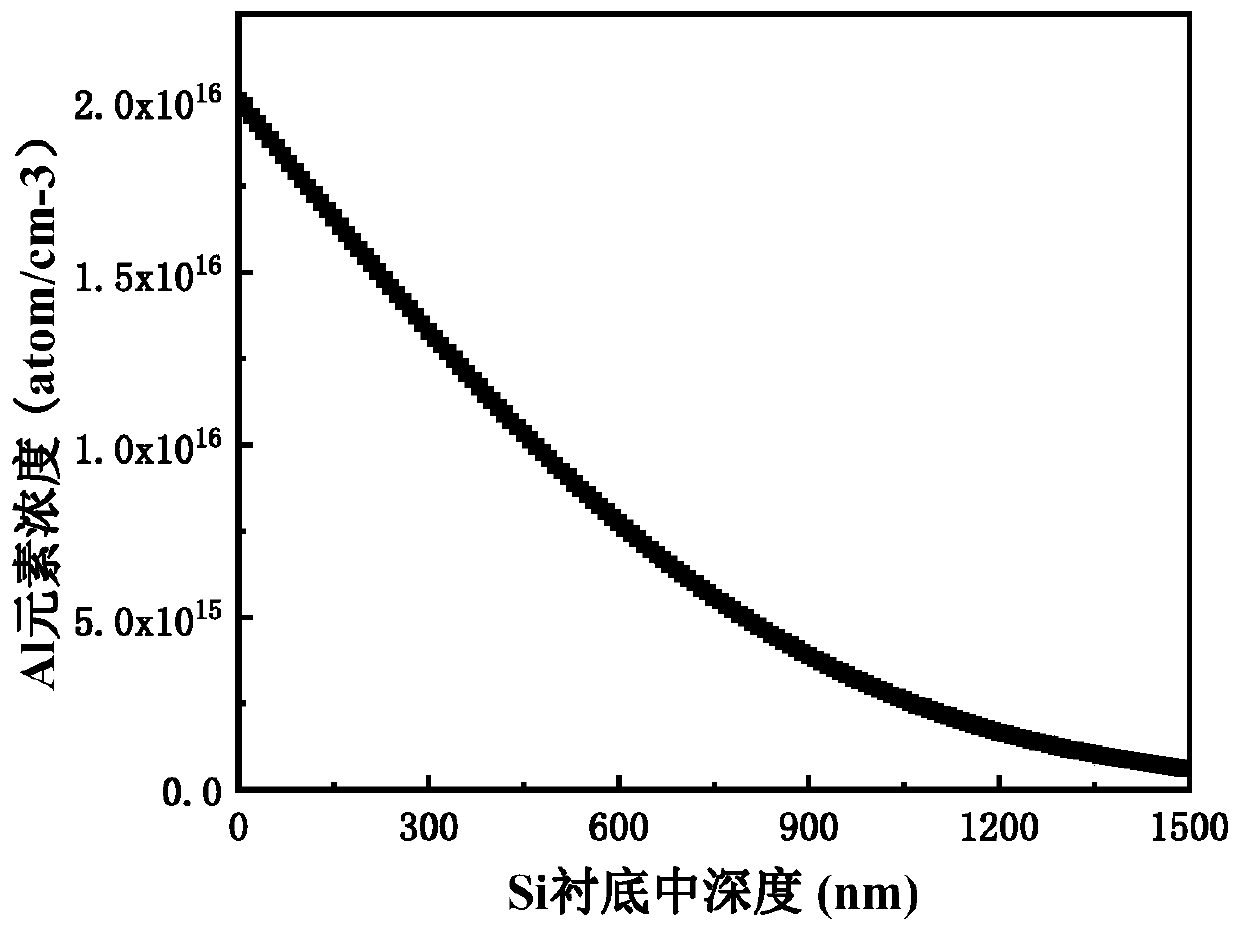
The aluminum nitride / silicon interface brought about by this layer of aluminum nitride is very critical for radio frequency loss. When growing this layer of aluminum nitride nucleation layer, aluminum atoms will diffuse into the silicon substrate, increasing the original high resistance silicon The conductivity of the substrate forms a p-type hole-conducting layer, which leads to a large RF loss in the microwave RF device in the studio

Method used


Image

  • Method for suppressing radio frequency loss of silicon-based gallium nitride radio frequency device
  • Method for suppressing radio frequency loss of silicon-based gallium nitride radio frequency device

Examples


Embodiment Construction

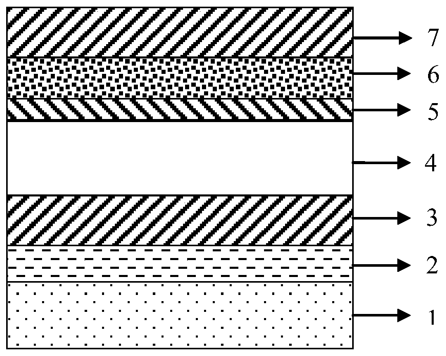
[0026] The key of the present invention is to perform pretreatment on the high-resistance silicon substrate in advance, and before epitaxial nitride, a layer of n-type single crystal silicon doped with phosphorus is epitaxially grown on the silicon substrate. The carrier concentration in single-crystal silicon needs to be controlled to match the estimated hole concentration distribution due to the diffusion of aluminum atoms.

[0027] Attached below figure 1 , the present invention will be further described by embodiment.

[0028] The structure of the silicon-based gallium nitride radio frequency device prepared in this embodiment is as follows figure 1 As shown, it includes a high-resistance silicon substrate and a phosphorus-doped n-type single-crystal silicon epitaxial layer 2, an aluminum nitride nucleation layer 3, an aluminum gallium nitrogen stress buffer layer 4, and a gallium nitride epitaxial layer sequentially stacked on the high-resistance silicon substrate. 5. A...


PUM

PropertyMeasurementUnit
thicknessaaaaaaaaaa
thicknessaaaaaaaaaa
thicknessaaaaaaaaaa

Abstract

The invention discloses a method for suppressing the radio frequency loss of a silicon-based gallium nitride radio frequency device. A layer of n-type monocrystalline silicon is arranged on a high-resistance silicon substrate in an epitaxial mode, so that a composite silicon substrate can be obtained; aluminum nitride and a subsequent gallium nitride film are arranged on the composite silicon substrate in an epitaxial mode; n-type electrons doped in the composite silicon substrate and hole flows brought by the diffusion of aluminum atoms are recombined, so that the silicon substrate is kept ina high-resistance state, and the radio frequency loss of the silicon-based gallium nitride radio frequency device is reduced. With the method adopted, the radio frequency loss of the device is effectively suppressed, the crystal quality of epitaxial layers is not reduced, the stability of the device is not influenced, operation is simple and quick, and cost is controllable.

Description

technical field [0001] The invention belongs to the technical field of semiconductors, and in particular relates to a method for suppressing the radio frequency loss problem faced by a silicon-based gallium nitride radio frequency device in application. Background technique [0002] The third-generation semiconductors represented by group III nitrides have excellent properties such as high band gap, high breakdown electric field, high saturation electron drift velocity, and strong polarization, especially based on silicon (Si) substrates and silicon carbide ( Aluminum gallium nitride / gallium nitride (AlGaN / GaN) heterostructure high mobility transistor (HEMT) on SiC substrate has excellent characteristics such as fast switching speed, low on-resistance, small device size, high temperature resistance, and energy saving. , is expected to be widely used in the field of next-generation microwave radio frequency power devices. [0003] At present, gallium nitride-based microwave ...

Claims


Application Information

Patent Timeline
Patent Type & Authority Applications(China)
IPC IPC(8): H01L29/06H01L29/778H01L21/02H01L21/335
CPCH01L21/02381H01L21/0245H01L21/02499H01L21/0254H01L29/0684H01L29/66462H01L29/7787
Inventor 杨学林沈波魏来马骋吴珊沈剑飞刘丹烁蔡子东黄华洋陈正昊
Owner PEKING UNIV
Learn More