
Method for manufacturing a p-doped grid in an n-doped sic layer

A technology of grid structure and doping concentration, which is applied in the manufacture of semiconductor/solid-state devices, semiconductor devices, electrical components, etc., can solve problems such as expensive, sharp trench grids, and complexity, so as to simplify manufacturing, avoid process, Avoid the effects of manufacturing steps

Pending Publication Date: 2020-05-22
ASCATRON AB
View PDF5 Cites 0 Cited by
  • Summary
  • Abstract
  • Description
  • Claims
  • Application Information

AI Technical Summary

Problems solved by technology

Disadvantages include: This is a complex process involving trench etch, epitaxial regrowth twice, and planarization with sub-micron precision and uniformity, which is very expensive
Fabrication of trench grids by combining trench etching and ion implantation also has the problem of sharp corners, where rounded corners must be etched

Method used


Image

  • Method for manufacturing a p-doped grid in an n-doped sic layer
  • Method for manufacturing a p-doped grid in an n-doped sic layer

Examples


Embodiment Construction

[0029] Before the present invention is disclosed and described in detail, it is to be understood that this invention is not limited to the particular compounds, configurations, method steps, substrates and materials disclosed herein as such compounds, configurations, method steps, substrates and materials may vary. It is also to be understood that the terminology used herein is for the purpose of describing particular embodiments only, and is not intended to be limiting, since the scope of the present invention will be limited only by the appended claims and their equivalents.

[0030] It must be noted that, as used in this specification and the appended claims, the singular forms "a," "an," and "the" include plural referents unless the context clearly dictates otherwise.

[0031] Unless otherwise defined, any terms and scientific terms used herein are intended to have the meaning commonly understood by one of ordinary skill in the art to which this invention belongs.

[0032]...


PUM

PropertyMeasurementUnit
thicknessaaaaaaaaaa
thicknessaaaaaaaaaa

Abstract

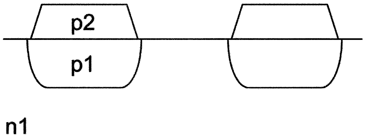
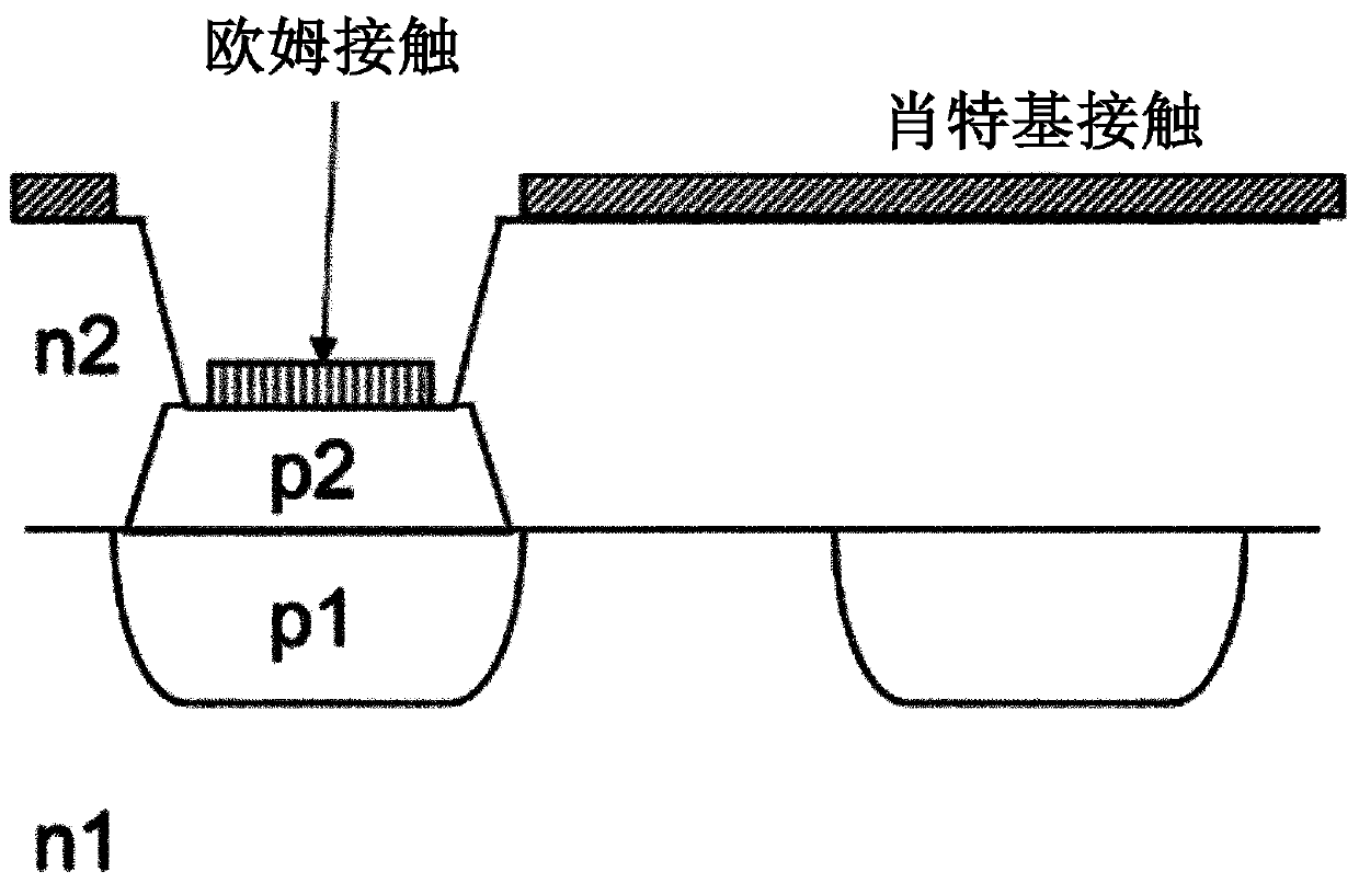
A grid is manufactured with a combination of ion implant and epitaxy growth. The grid structure is made in a SiC semiconductor material with the steps of a) providing a substrate comprising a doped semiconductor SiC material, said substrate comprising a first layer (n1), b) by epitaxial growth adding at least one doped semiconductor SiC material to form separated second regions (p2) on the first layer (n1), if necessary with aid of removing parts of the added semiconductor material to form separated second regions (p2) on the first layer (n1), and c) by ion implantation at least once at a stage selected from the group consisting of directly after step a), and directly after step b); implanting ions in the first layer (n1) to form first regions (p1). It is possible to manufacture a grid with rounded corners as well as an upper part with a high doping level. It is possible to manufacture a component with efficient voltage blocking, high current conduction, low total resistance, high surge current capability, and fast switching.

Description

technical field [0001] The present invention relates to a cost-effective method of fabricating an improved grid structure by combining ion implantation and epitaxial growth. The grid can be a buried grid or a surface grid. Background technique [0002] Embedded doped structures or buried grids (BGs) can be used to confine the electric field at the surface of the power semiconductor, thereby shielding electric field sensitive areas (such as Schottky contacts or MOS structures) from high electric fields in the drift layer. This is especially important for devices based on wide bandgap semiconductors such as SiC, where the electric field in the device drift layer can be 10 times higher than in silicon. Therefore, confinement at the semiconductor surface or with gate oxides like (SiO 2 ) like other materials where the electric field at the interface is important, this material can withstand a much lower critical electric field than semiconductors. [0003] According to the cu...

Claims


Application Information

Patent Timeline
Patent Type & Authority Applications(China)
IPC IPC(8): H01L21/329H01L21/337H01L29/808H01L29/872H01L29/739H01L29/78H01L29/06H01L29/16H01L29/36H01L29/10
CPCH01L29/36H01L29/6606H01L29/66068H01L29/7395H01L29/8083H01L29/872H01L29/0623H01L29/1066H01L29/1608H01L21/02167H01L21/02447H01L21/02529H01L29/0619H01L21/02634H01L21/26513H01L21/28537H01L21/30625H01L21/3065H01L21/324H01L29/401H01L29/402H01L21/046
Inventor 阿道夫·舍纳谢尔盖·雷沙诺夫尼古拉斯-蒂埃里·杰巴里侯赛因·伊莱希帕纳
Owner ASCATRON AB
Learn More