Three-dimensional memory and preparation method thereof

A memory, three-dimensional technology, applied in the semiconductor field, can solve the problems affecting the electrical performance of the three-dimensional memory, the reduction of the yield of the three-dimensional memory, and the height of the gate gap stack, so as to reduce the risk of tilt, improve the contour distortion, and improve the electrical performance.

Inactive Publication Date: 2020-05-15
YANGTZE MEMORY TECH CO LTD
View PDF4 Cites 5 Cited by
  • Summary
  • Abstract
  • Description
  • Claims
  • Application Information

AI Technical Summary

Problems solved by technology

[0003] In view of this, the present application provides a three-dimensional memory and its preparation method to solve the problem of high gate gap stacking height and serious tilt risk in the etching process in the prior art, which leads to the process of filling the gate metal in the subsequent word line opening. It is easy to generate leakage current, which affects the electrical performance of the three-dimensional memory, and then leads to the problem that the yield rate of the three-dimensional memory is reduced

Method used


Image

  • Three-dimensional memory and preparation method thereof
  • Three-dimensional memory and preparation method thereof
  • Three-dimensional memory and preparation method thereof

Examples


Embodiment Construction

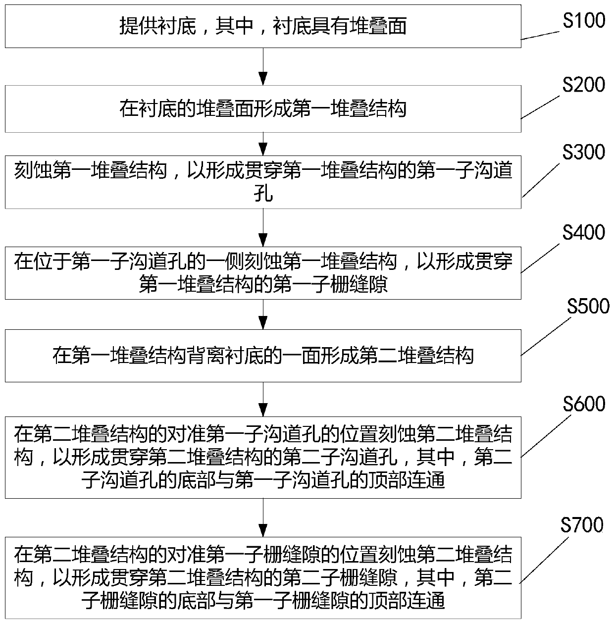
[0049] Specific embodiments of the present invention will be described in more detail below with reference to the accompanying drawings. Although exemplary embodiments of the invention are shown in the drawings, it should be understood that the invention may be practiced in other ways than those described herein, and therefore, the invention is not limited by the following embodiments.

[0050] A three-dimensional (3D) memory is mainly used as a non-volatile flash memory. The two main non-volatile flash memory technologies use NAND (NAND) and NOR (NOR) structures. Compared with NOR memory, the writing speed in NAND memory is fast, the erasing operation is simple, and smaller memory cells can be realized, thereby achieving higher storage density. Therefore, the 3D memory using the NAND structure has been widely used.

[0051] With the increase of the number of layers and the stack height in the three-dimensional NAND memory, in order to increase the storage density, a high as...


PUM


Abstract

The invention provides a three-dimensional memory and a preparation method thereof. The preparation method comprises the following steps: providing a substrate, and forming a first stacking structureon the stacking surface of the substrate; etching the first stacked structure to form a first sub-channel hole penetrating through the first stacked structure; etching the first stacking structure onone side of the first sub-channel hole to form a first sub-gate gap penetrating through the first stacking structure; forming a second stacking structure on one surface, deviating from the substrate,of the first stacking structure; etching the second stacking structure at the position, aligned with the first sub-channel hole, of the second stacking structure to form a second sub-channel hole penetrating through the second stacking structure; and etching the second stacked structure at a position, aligned with the first sub-gate gap, of the second stacked structure to form a second sub-gate gap penetrating through the second stacked structure. The preparation method provided by the invention solves the problem that the electrical performance and yield of the three-dimensional memory are influenced due to high gate gap stacking height, serious inclination risk and easy generation of leakage current in an etching process in the prior art.

Description

technical field [0001] The invention relates to the technical field of semiconductors, in particular to a three-dimensional memory and a preparation method thereof. Background technique [0002] At present, in the preparation process of a three-dimensional memory, a substrate is generally provided first and a stacked structure is formed on the substrate, and then a channel hole (Channel hole, CH) is first formed in the stacked structure, and the channel hole is formed in the stacked structure. A gate line slit (Gate line slit, GLS) is formed after the hole, so as to form a word line opening by removing the sacrificial layer in the stacked structure through the gate line slit, and prepare for subsequent filling of gate metal in the word line opening and other processes. However, in the process of forming gate gaps through an etching process, it is difficult to etch along a predetermined direction perpendicular to the semiconductor substrate, but it will be inclined, and the d...

Claims


Application Information

Patent Timeline
Patent Type & Authority Applications(China)
IPC IPC(8): H01L27/11563H01L27/11568H01L27/11578
CPCH10B43/00H10B43/30H10B43/20
Inventor 殷姿杨川许波谢柳群吴智鹏张璐刘思敏
Owner YANGTZE MEMORY TECH CO LTD
Why Eureka
Try Eureka