


Quick Research
Generate reliable direction feasibility study reports for your R&D in just a few steps.

Technical Q&A
Discover and master advanced knowledge NOW. Basics, ideas, possibilities, all at once.

Find Solutions
As an expert in R&D theories, this can generate solutions to your technical problems instantly.

Evaluate Feasibility
Analyze your overall solution with one click, know your potential R&D risks in advance.

Monitor Landscape
Get weekly tech updates, stay abreast of the latest tech innovations and key insights.
Light-emitting device capable of being circularly prepared and preparation method
A light-emitting device, recycling preparation technology, applied in the manufacture/processing of organic light-emitting devices, organic light-emitting devices, semiconductor/solid-state device manufacturing, etc., can solve the problems of lack of research on the recycling of electroluminescent devices, and achieve rich raw materials and methods Simplicity and the effect of reducing the production cost
- Summary
- Abstract
- Description
- Claims
- Application Information
AI Technical Summary
Problems solved by technology
Method used
Image

Examples
Embodiment 1
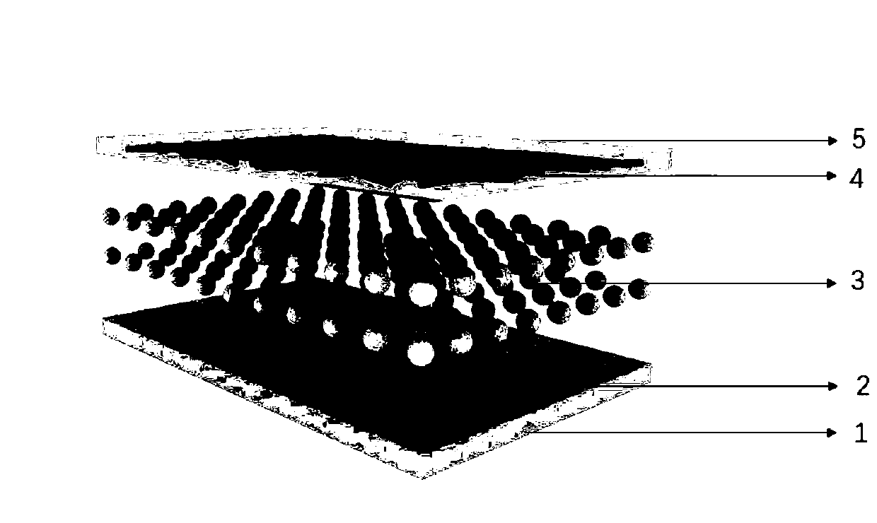
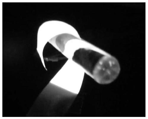
[0043] Such as figure 1 Shown is a structure diagram of a light-emitting thin film device, which includes a polymer substrate 1 , a bottom electrode 2 , a light-emitting functional layer 3 , a top electrode 4 , and an insulating polymer protective layer 5 .
[0044] The polymer substrate 1 is a transparent or translucent non-water-soluble insulating polymer; the bottom electrode 2 is a silver nanowire conductive film; the light-emitting functional layer 3 is a mixture of phosphor powder and a transparent water-soluble insulating polymer or a translucent water-soluble insulating polymer compound; the top electrode 4 is a silver nanowire conductive film; the insulating encapsulation layer 5 is a transparent or translucent non-water-soluble insulating polymer.
[0045] The top and bottom electrodes are both silver nanowire conductive films, the sheet resistance thereof is 1Ω / sq-1000Ω / sq, and the light transmittance is 40%-100%. The average length of the silver wires in the silve...
Embodiment 2
[0058] Such as figure 1 Shown is a structure diagram of a light-emitting thin film device, which includes a polymer substrate 1 , a bottom electrode 2 , a light-emitting functional layer 3 , a top electrode 4 , and an insulating polymer protective layer 5 .
[0059] The polymer substrate 1 is a transparent or translucent non-water-soluble insulating polymer; the bottom electrode 2 is a silver nanowire conductive film; the light-emitting functional layer 3 is a mixture of phosphor powder and a transparent water-soluble insulating polymer or a translucent water-soluble insulating polymer compound; the top electrode 4 is a silver nanowire conductive film; the insulating encapsulation layer 5 is a transparent or translucent non-water-soluble insulating polymer.
[0060] The average length of the silver nanowires used in the preparation method of the light-emitting device of this embodiment is 20 μm.
[0061] 1) Preparation of the top electrode: Spray silver nanowire ethanol solut...
Embodiment 3
[0067] Such as figure 1 Shown is a structure diagram of a light-emitting thin film device, which includes a polymer substrate 1 , a bottom electrode 2 , a light-emitting functional layer 3 , a top electrode 4 , and an insulating polymer protective layer 5 .
[0068] The polymer substrate 1 is a transparent or translucent non-water-soluble insulating polymer; the bottom electrode 2 is a silver nanowire conductive film; the light-emitting functional layer 3 is a mixture of phosphor powder and a transparent water-soluble insulating polymer or a translucent water-soluble insulating polymer compound; the top electrode 4 is a silver nanowire conductive film; the insulating encapsulation layer 5 is a transparent or translucent non-water-soluble insulating polymer.
[0069] In the preparation method of the light-emitting device in this example, the average length of silver nanowires is 30 μm.
[0070] 1) Preparation of the top electrode: Spray silver nanowire ethanol solution on the ...
PUM
| Property | Measurement | Unit |
|---|---|---|
| length | aaaaa | aaaaa |
| length | aaaaa | aaaaa |
| length | aaaaa | aaaaa |
Abstract
Description
Claims
Application Information
 - R&D Engineer
- R&D Manager
- IP Professional
- Industry Leading Data Capabilities
- Powerful AI technology
- Patent DNA Extraction
Browse by: Latest US Patents, China's latest patents, Technical Efficacy Thesaurus, Application Domain, Technology Topic, Popular Technical Reports.
© 2024 PatSnap. All rights reserved.Legal|Privacy policy|Modern Slavery Act Transparency Statement|Sitemap|About US| Contact US: help@patsnap.com