A kind of integrated circuit package and its preparation method

An integrated circuit and package technology, applied in the field of integrated circuit package and its preparation, can solve the problems of open circuit of solder joints and failure of integrated circuit package, so as to improve the yield, ensure high consistency and reduce the probability of open circuit. Effect

Active Publication Date: 2021-07-13
NANTONG FUJITSU MICROELECTRONICS
View PDF3 Cites 0 Cited by
  • Summary
  • Abstract
  • Description
  • Claims
  • Application Information

AI Technical Summary

Problems solved by technology

[0003] The inventors of the present application have found in the long-term research process that during the reflow soldering process of the above-mentioned integrated circuit package, due to the warpage of the substrate or the tilt of the chip during mounting, the solder balls on the chip may not match the solder balls at the corresponding positions. The second pad on the substrate is connected, which leads to an open circuit of the solder joint, which makes the IC package fail

Method used


Image

  • A kind of integrated circuit package and its preparation method
  • A kind of integrated circuit package and its preparation method
  • A kind of integrated circuit package and its preparation method

Examples


Embodiment Construction

[0027] The following will clearly and completely describe the technical solutions in the embodiments of the present application with reference to the drawings in the embodiments of the present application. Obviously, the described embodiments are only some of the embodiments of the present application, not all of them. Based on the embodiments in this application, all other embodiments obtained by persons of ordinary skill in the art without making creative efforts belong to the scope of protection of this application.

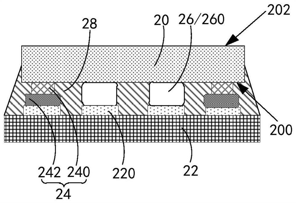
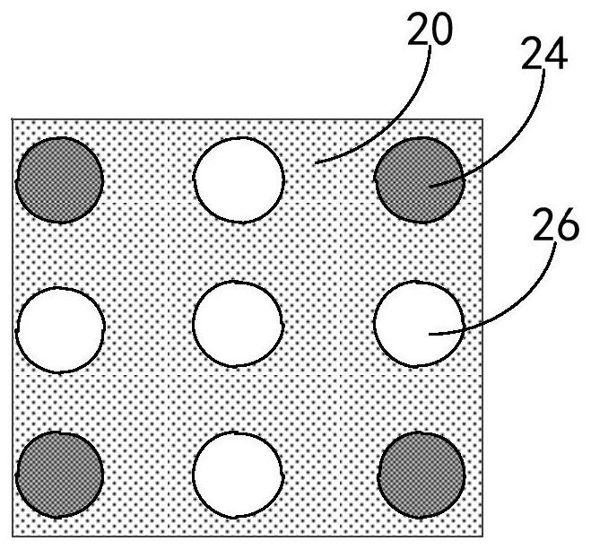
[0028] see figure 1 , figure 1 It is a structural schematic diagram of an embodiment corresponding to the manufacturing method of the integrated circuit package in the prior art. Such as figure 1 As shown in a, balls are normally planted on the first pad (not shown) on the functional surface 100 of the chip 10, and all solder balls 102 can be planted at one time; figure 1 As shown in b, the chip 10 is flip-chip mounted on the substrate 12, and the solder ba...


PUM


Abstract

The application provides an integrated circuit package and its preparation method. The package includes: a chip, including a functional surface and a non-functional surface oppositely arranged, and a plurality of first pads arranged at intervals are arranged on the functional surface The substrate is arranged at a distance from the chip, and the substrate is provided with a second pad at a position corresponding to the first pad; a plurality of first soldering bodies, including a conductive support and at least one of the conductive supports The first solder layer at one end of one side, the first solder body is electrically connected between part of the first pad and the corresponding second pad; a plurality of second solder bodies, including the second solder layer, and the second soldering body is electrically connected between the remaining first pad and the corresponding second pad; wherein, the melting point of the conductive support is higher than that of the first solder layer and the first solder layer. The melting point of the second solder layer. Through the above method, the present application can reduce the probability of the chip being tilted relative to the substrate during reflow.

Description

technical field [0001] The present application relates to the field of packaging technology, in particular to an integrated circuit package and a preparation method thereof. Background technique [0002] Among integrated circuit packages, ball array packaging is a relatively common product packaging method. The packaging method specifically includes: using a ball planting machine to form solder balls on the first pad of the chip, and then using surface mount technology to mount and reflow solder the chip and the substrate. [0003] The inventors of the present application have found in the long-term research process that during the reflow soldering process of the above-mentioned integrated circuit package, due to the warpage of the substrate or the tilt of the chip during mounting, the solder balls on the chip may not match the solder balls at the corresponding positions. The second pad on the substrate is connected, thereby causing an open circuit of the solder joint, so t...

Claims


Application Information

Patent Timeline
Patent Type & Authority Patents(China)
IPC IPC(8): H01L23/488H01L21/60
CPCH01L24/16H01L24/81H01L2224/16238H01L2224/16501H01L2224/8121H01L2224/73204H01L2224/81
Inventor 周锋
Owner NANTONG FUJITSU MICROELECTRONICS
Why Eureka
Try Eureka