Modular multi-chip packaging structure and packaging method thereof

A technology of multi-chip packaging and packaging method, which is applied in the direction of semiconductor/solid-state device components, semiconductor devices, electrical components, etc., can solve the problems of electrical performance loss, chip splits, etc., and reduce electrical loss and packaging volume , the effect of avoiding losses

Active Publication Date: 2020-04-24
华天科技(南京)有限公司
View PDF8 Cites 0 Cited by
  • Summary
  • Abstract
  • Description
  • Claims
  • Application Information

AI Technical Summary

Problems solved by technology

[0002] With the development of the semiconductor packaging industry, a multi-chip stacking technology has been used in the packaging of storage products to provide the package with a larger capacity for storing or executing data. The stacking method is superimposed to achieve expansion. The chips of each layer are directly interconnected through wire bond bonding. This method generally requires thinner chip thickness and the bonding wires are suspended, which is easy to cause chip cracks, and longer wire bond bonding is also loss of electrical performance

Method used


Image

  • Modular multi-chip packaging structure and packaging method thereof
  • Modular multi-chip packaging structure and packaging method thereof
  • Modular multi-chip packaging structure and packaging method thereof

Examples


Embodiment Construction

[0028] The present invention is described in further detail below in conjunction with accompanying drawing:

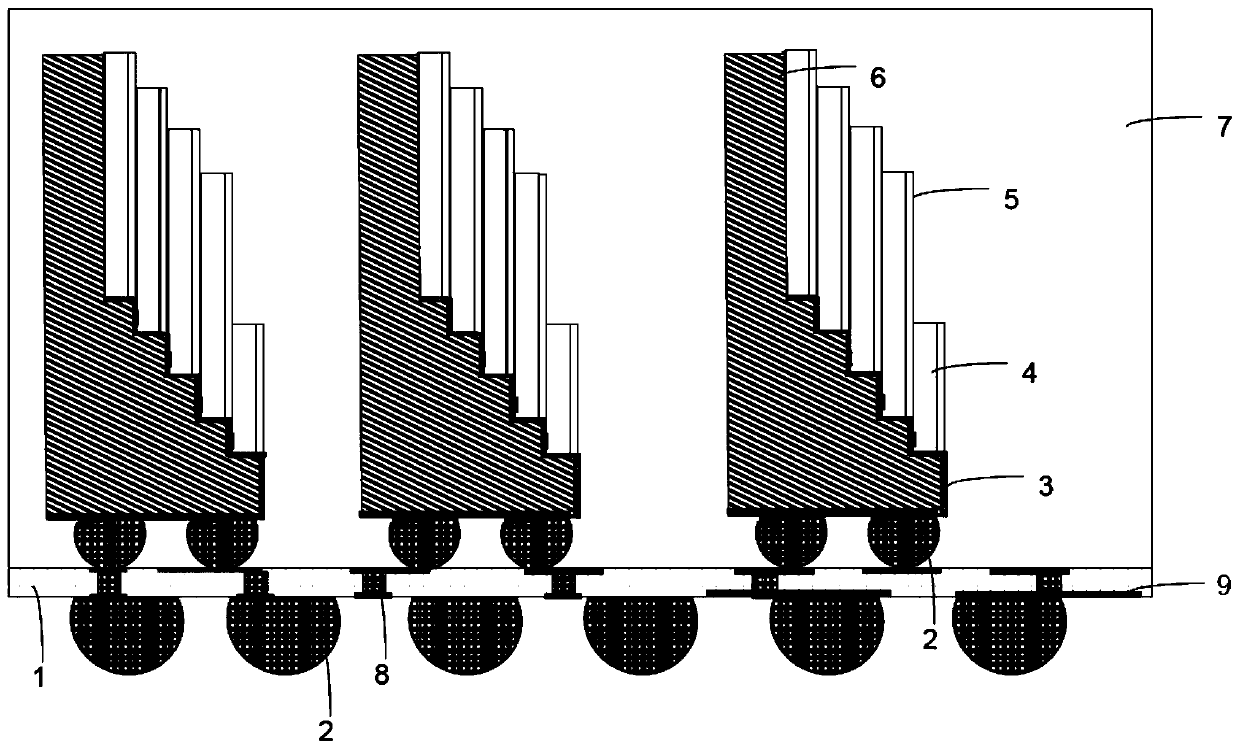
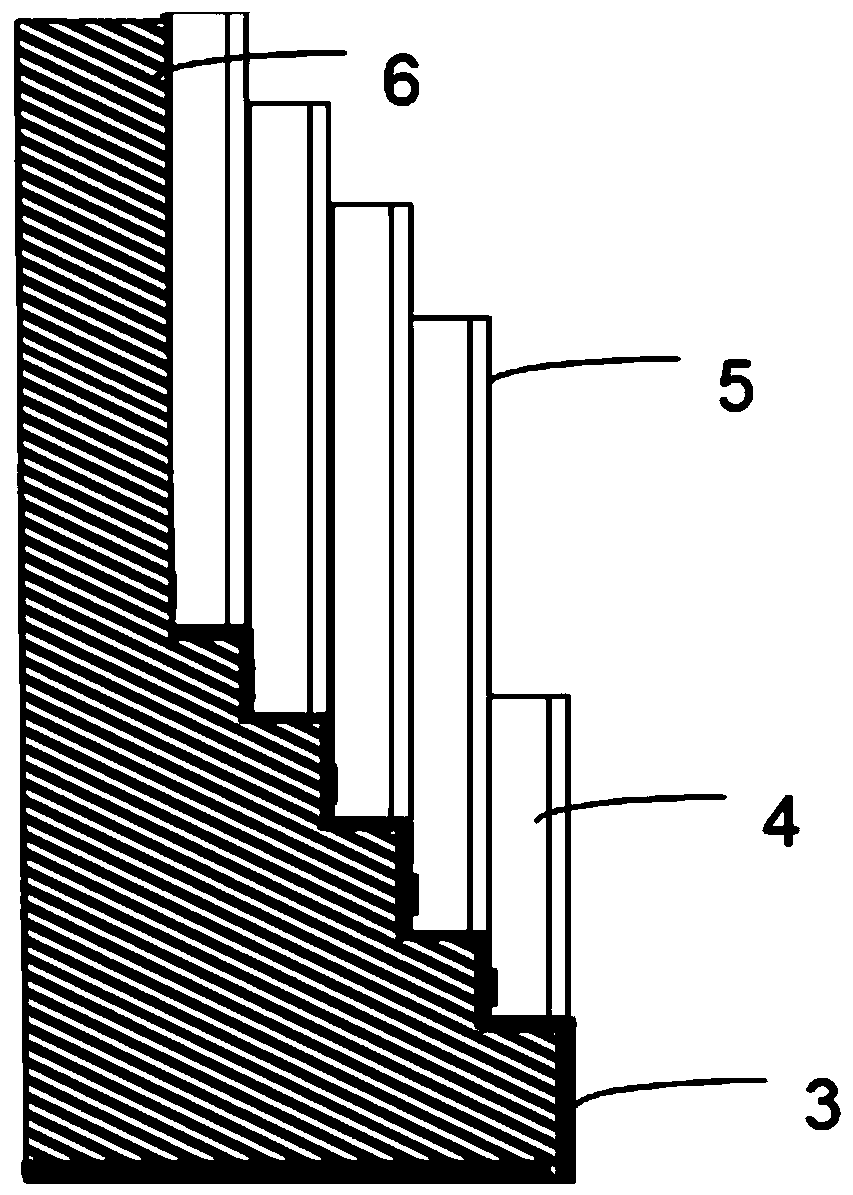
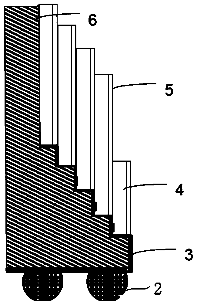
[0029] see Figure 1 to Figure 5 As shown, a modular multi-chip packaging structure includes a substrate 1 and a plurality of packaging units arrayed on the substrate 1, the packaging unit includes a plurality of chips 4 stacked in steps, and the lead ends of the plurality of chips 4 pass through the chip wiring 3 Connection, the step surface on one side of the lead end of multiple chips 4 is plastic-sealed by the first plastic package 6, and the bottom of the first plastic package 6 is provided with an etching circuit connected to the chip wiring 3; The etched circuit at the bottom is connected to the connection wiring on the substrate 1 , the chip 4 is vertically arranged on the substrate 1 after plastic packaging, and multiple packaging units are plastic-sealed on the substrate 1 through the second plastic packaging body 7 . The lead ends of the chips 4 stacked in ...


PUM


Abstract

The invention discloses a modular multi-chip packaging structure and a packaging method thereof. A plurality of packaging units arrayed on a substrate are packaging units formed by a plurality of chips which are stacked in a stepped manner. The lead ends of the chips stacked in a stepped manner are positioned on the surfaces of the steps, and the lead ends of the plurality of chips are connected through chip wiring. Chip routing is not needed, the packaging volumes of the chips are reduced, and the loss of the electrical property on a wire bond line is avoided. Plastic packaging is carried outon the step surfaces on one sides of the lead ends of the plurality of chips through a first plastic packaging body. An etching circuit connected with the chip wiring is arranged at the bottom of thefirst plastic packaging body, connection wiring is arranged on the substrate, and the etching circuit at the bottom of the first plastic packaging body is connected with the connection wiring on thesubstrate. Finally, the plurality of packaging units are packaged on the substrate through a second plastic packaging body, and the chips are vertically arranged on the substrate after plastic packaging. Different functions can be integrated by packaging the independent modules together, the limitation of traditional multi-chip packaging is well broken through, the structure is simple, and the connection is stable.

Description

【Technical field】 [0001] The invention belongs to the technical field of storage chip packaging, and in particular relates to a modular multi-chip packaging structure and a packaging method thereof. 【Background technique】 [0002] With the development of the semiconductor packaging industry, a multi-chip stacking technology has been used in the packaging of storage products to provide the package with a larger capacity for storing or executing data. The stacking method is superimposed to achieve expansion. The chips of each layer are directly interconnected through wire bond bonding. This method generally requires thinner chip thickness and the bonding wires are suspended, which is easy to cause chip cracks, and longer wire bond bonding is also There will be a loss of electrical performance. Therefore, for this packaging method, higher integration and reliability are crucial. 【Content of invention】 [0003] The object of the present invention is to overcome the disadvant...

Claims


Application Information

Patent Timeline
IPC IPC(8): H01L23/31H01L23/498H01L23/488H01L21/56H01L21/60
CPCH01L23/49838H01L23/49816H01L23/3128H01L23/3185H01L23/3171H01L24/32H01L24/24H01L21/56H01L24/82H01L2224/32145H01L2224/24145
Inventor 董晨马晓建杨巧
Owner 华天科技(南京)有限公司
Why Eureka
Try Eureka