


Quick Research
Generate reliable direction feasibility study reports for your R&D in just a few steps.

Technical Q&A
Discover and master advanced knowledge NOW. Basics, ideas, possibilities, all at once.

Find Solutions
As an expert in R&D theories, this can generate solutions to your technical problems instantly.

Evaluate Feasibility
Analyze your overall solution with one click, know your potential R&D risks in advance.

Monitor Landscape
Get weekly tech updates, stay abreast of the latest tech innovations and key insights.
Plating device
An electroplating device and catholyte technology, which is applied in current insulation devices, electrophoretic plating, plating baths, etc., can solve the problems of difficulty in controlling the electric field and the uniformity of the electrolyte, so as to improve the electroplating rate, improve the uniformity, improve the The effect of traffic
- Summary
- Abstract
- Description
- Claims
- Application Information
AI Technical Summary
Problems solved by technology
Method used
Image

Examples
Embodiment Construction
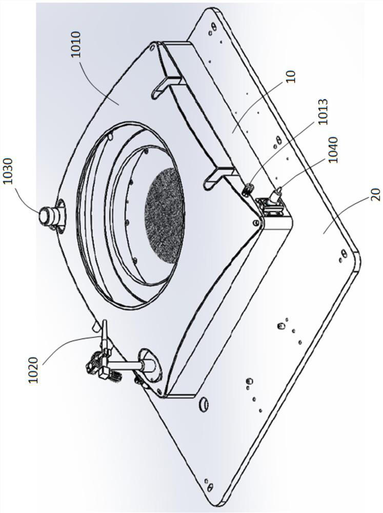
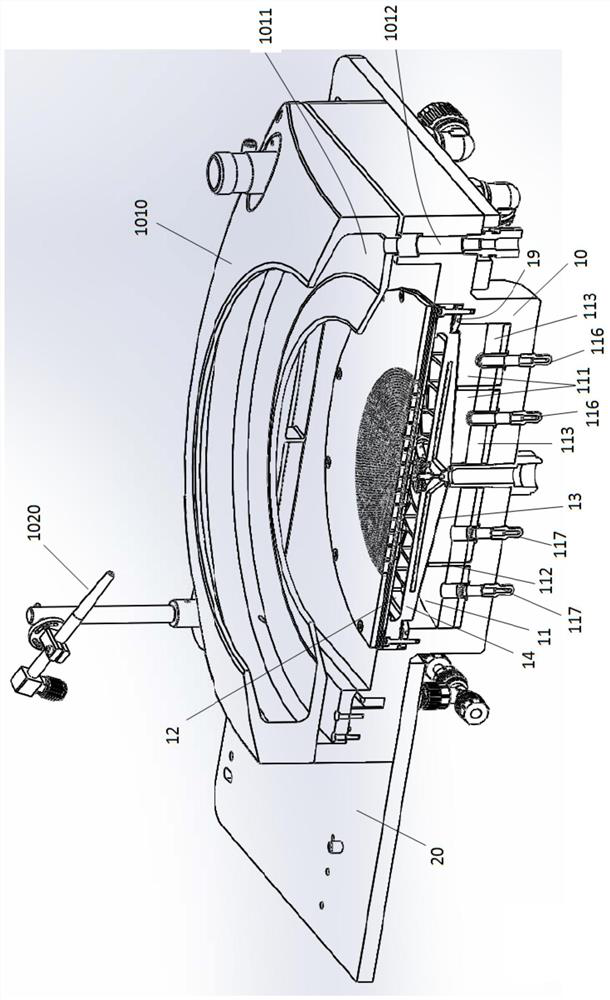
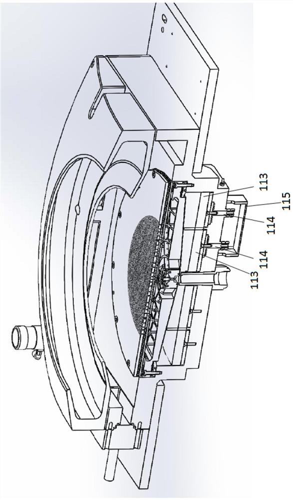
[0034] refer to Figure 1 to Figure 7 As shown, an electroplating device according to an exemplary embodiment of the present invention is disclosed. The electroplating device includes a process chamber 10 . The process chamber 10 is supported by a susceptor 20 . The process chamber 10 is divided into an anode chamber 11 and a cathode chamber 12 . The anode cavity 11 and the cathode cavity 12 are separated by a membrane 13 fixed on a membrane frame 14 .
[0035] The anode cavity 11 is divided into a plurality of anode regions 111 and every two adjacent anode regions 111 are separated by partition walls 112 arranged vertically. The material of the partition wall 112 can be selected from non-conductive and chemically resistant plastics. Partition wall 112 separates the electric field and confines the electrolyte fluid field. In one embodiment, by way of example, without limiting the invention, the anode cavity 11 is divided into two anode regions 111 . Each anode area 111 a...
PUM
 Abstract
Description
Claims
Application Information
 - R&D Engineer
- R&D Manager
- IP Professional
- Industry Leading Data Capabilities
- Powerful AI technology
- Patent DNA Extraction
Browse by: Latest US Patents, China's latest patents, Technical Efficacy Thesaurus, Application Domain, Technology Topic, Popular Technical Reports.
© 2024 PatSnap. All rights reserved.Legal|Privacy policy|Modern Slavery Act Transparency Statement|Sitemap|About US| Contact US: help@patsnap.com