Perovskite solar cell based on nano grass-shaped mesoporous layer and preparation method thereof
A solar cell and perovskite technology, applied in nanotechnology, circuits, photovoltaic power generation, etc., can solve problems such as limiting development, achieve enhanced transmission and extraction, improved performance, and low cost
- Summary
- Abstract
- Description
- Claims
- Application Information
AI Technical Summary
Problems solved by technology
Method used
Image
Examples
Embodiment 1
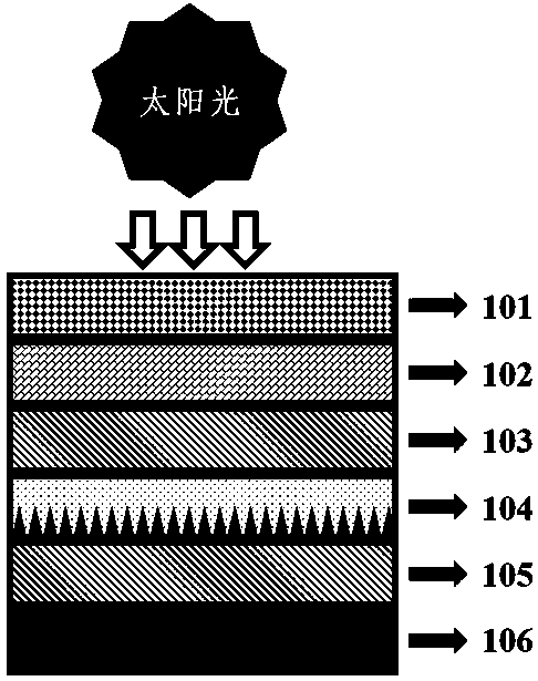
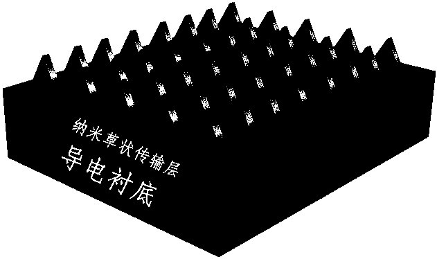
[0031] The structure of a high-efficiency perovskite solar cell based on nanograss-like mesoporous layers figure 1 As shown: 101 is a transparent substrate, 102 is a first electrode layer, 103 is an electron transport layer, 104 is a perovskite light absorption layer, 105 is a hole transport layer, and 106 is a second electrode layer. The transparent substrate is quartz glass; the first transparent electrode layer is ITO with a thickness of 180 nm; the electron transport layer is high-energy 001-face sheet-like single-crystal nanograss structure TiO 2 , with a thickness of 80 nm; the perovskite layer is Cs 0.05 (MA 0.13 FA 0.87 ) 0.95 Pb(I 0.87 Br 0.13 ) 3 , with a thickness of 450 nm; the hole transport layer is Spiro-OMeTAD with a thickness of 100 nm; the second electrode layer is gold with a thickness of 80 nm.
[0032] The preparation method of the perovskite solar cell in embodiment 1 is as follows:
[0033] ITO conductive glass is cleaned with glass cleaning solu...
Embodiment 2
[0035] The structure of a high-efficiency perovskite solar cell based on nanograss-like mesoporous layers is as follows from bottom to top: transparent substrate, first electrode layer, hole transport layer, perovskite light absorption layer, electron transport layer, second electrode layer. The transparent substrate is quartz glass; the first transparent electrode layer is ITO with a thickness of 180nm; the hole transport layer is flaky single crystal nanograss NiO x , with a thickness of 40 nm; the perovskite layer is Cs 0.05 (MA 0.13 FA 0.87 ) 0.95 Pb(I 0.87 Br 0.13 ) 3 , with a thickness of 450 nm; the electron transport layer is PCBM with a thickness of 50 nm; the second electrode layer is silver with a thickness of 80 nm.
[0036] The preparation method of the perovskite solar cell in embodiment 2 is as follows:
[0037] The ITO conductive glass is cleaned with glass cleaning solution, acetone, and ethanol in sequence, and after drying, the residual organic matte...
PUM
| Property | Measurement | Unit |
|---|---|---|
| thickness | aaaaa | aaaaa |
| thickness | aaaaa | aaaaa |
| thickness | aaaaa | aaaaa |
Abstract
Description
Claims
Application Information
 - R&D
- Intellectual Property
- Life Sciences
- Materials
- Tech Scout
- Unparalleled Data Quality
- Higher Quality Content
- 60% Fewer Hallucinations
Browse by: Latest US Patents, China's latest patents, Technical Efficacy Thesaurus, Application Domain, Technology Topic, Popular Technical Reports.
© 2025 PatSnap. All rights reserved.Legal|Privacy policy|Modern Slavery Act Transparency Statement|Sitemap|About US| Contact US: help@patsnap.com


