Circuit for accurately correcting duty ratio of clock signal
A technology of clock signal and duty cycle, which is applied in the direction of transforming continuous pulse chains into pulse chain devices with required modes, and can solve problems such as consumption, large current, and occupancy
- Summary
- Abstract
- Description
- Claims
- Application Information
AI Technical Summary
Problems solved by technology
Method used
Image
Examples
Embodiment Construction
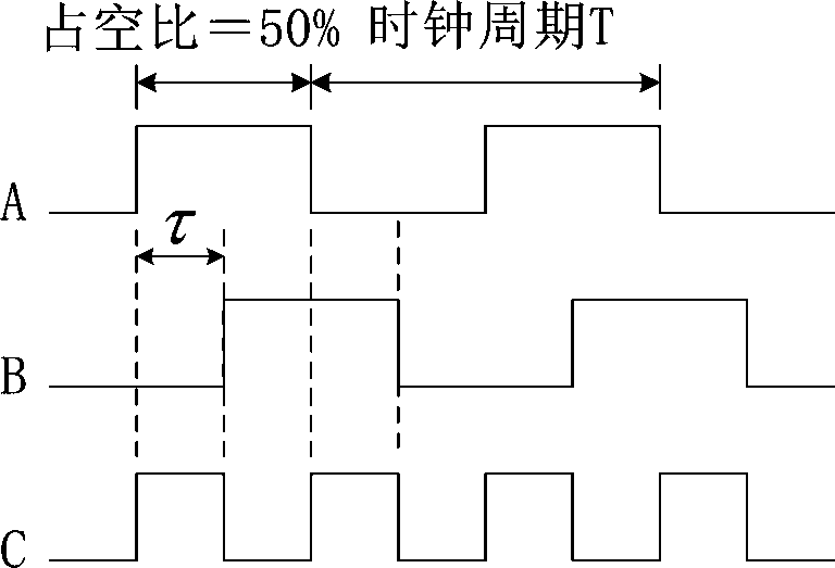
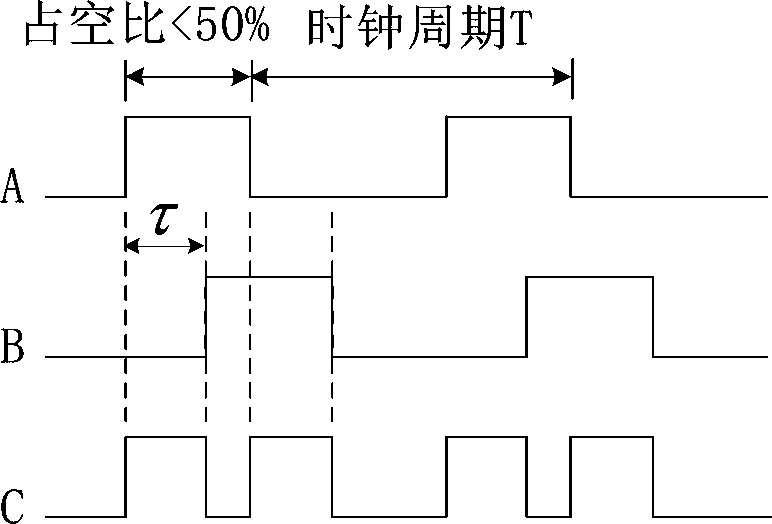
[0059] see Figure 9 , which is Embodiment 1 of the clock signal duty ratio correction circuit provided in this application. The clock signal duty ratio correction circuit 100 includes an inverter chain 110 , a delay unit 120 , a phase detection unit 130 and a low-pass filter 140 . The input signal CLKIN is input to the input end of the inverter chain 110, and the duty ratio of the input signal CLKIN is adjusted by changing the gate bias voltage of the first CMOS inverter in the inverter chain 110, and the inverter chain 110 outputs the output signal CLKOUT after the duty ratio correction to the outside. The output signal CLKOUT passes through the delay unit 120 to obtain a delayed signal, and the output terminal of the delay unit 120 is called a node VC. The output signal CLKOUT and the delay signal are used as the input of the phase detection unit 130. The phase detection unit 130 outputs an indication signal representing whether the duty ratio of the output signal CLKOUT ...
PUM
 Abstract
Description
Claims
Application Information
 - R&D
- Intellectual Property
- Life Sciences
- Materials
- Tech Scout
- Unparalleled Data Quality
- Higher Quality Content
- 60% Fewer Hallucinations
Browse by: Latest US Patents, China's latest patents, Technical Efficacy Thesaurus, Application Domain, Technology Topic, Popular Technical Reports.
© 2025 PatSnap. All rights reserved.Legal|Privacy policy|Modern Slavery Act Transparency Statement|Sitemap|About US| Contact US: help@patsnap.com


