
Wafer, wafer detection system and wafer detection method

A detection method and detection system technology, applied in the direction of semiconductor/solid-state device testing/measurement, single semiconductor device testing, electrical components, etc., can solve problems such as time-consuming, accidental damage of micro light-emitting diodes, etc., to speed up and improve detection efficiency Effect

Active Publication Date: 2020-03-31
PLAYNITRIDE DISPLAY CO LTD
View PDF3 Cites 0 Cited by
  • Summary
  • Abstract
  • Description
  • Claims
  • Application Information

AI Technical Summary

Problems solved by technology

However, due to the large number of micro-LEDs in the wafer, it takes considerable time to inspect each micro-LED in the wafer one by one, or to inspect some of the micro-LEDs in the wafer.
In addition, because the size of the micro-LEDs is on the order of microns, it is easy to cause accidental damage to the micro-LEDs when a probe is used to touch the electrodes of the micro-LEDs

Method used


Image

  • Wafer, wafer detection system and wafer detection method
  • Wafer, wafer detection system and wafer detection method
  • Wafer, wafer detection system and wafer detection method

Examples


Embodiment Construction

[0031] The aforementioned and other technical contents, features and effects of the present application will be clearly presented in the following detailed description of a preferred embodiment with reference to the accompanying drawings. The directional terms mentioned in the following embodiments, such as: up, down, left, right, front or back, etc., are only referring to the directions of the drawings. Accordingly, the directional terms used are for illustration and not for limitation of the application.

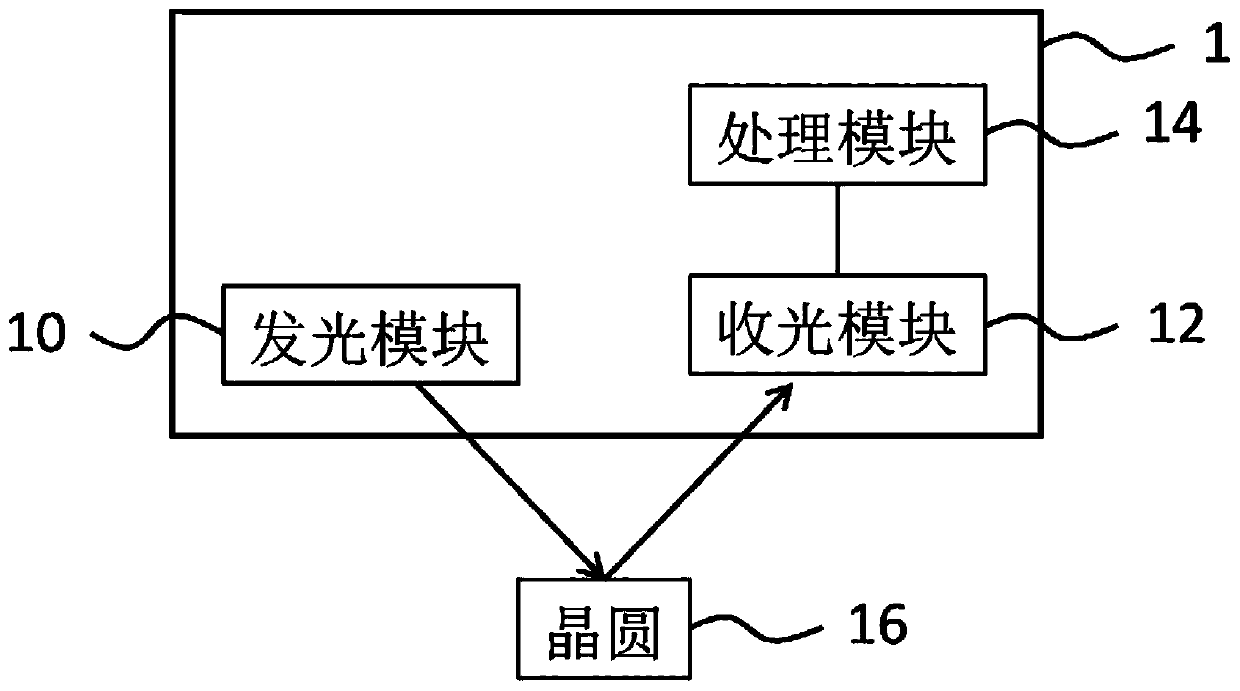
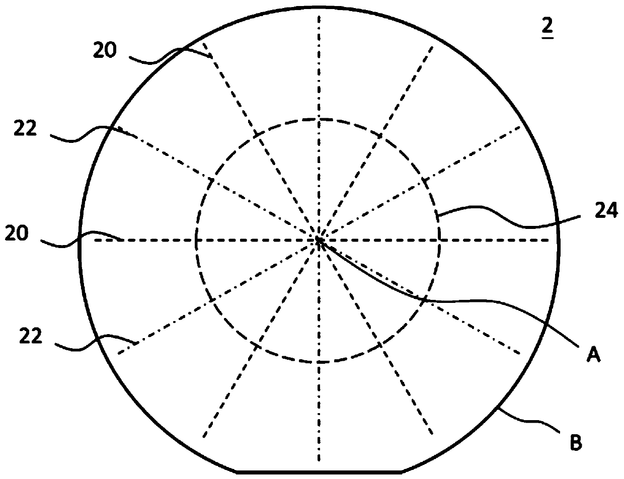
[0032] see Figure 1A and Figure 1B , Figure 1A is a functional block diagram illustrating a wafer inspection system according to an embodiment of the present application, Figure 1B is a schematic diagram illustrating the structure of a wafer according to an embodiment of the present application. As shown in the figure, the wafer inspection system 1 disclosed in this embodiment can be used to inspect the quality of a wafer 16 , and the wafer inspection system 1 can in...


PUM

PropertyMeasurementUnit
wavelengthaaaaaaaaaa

Abstract

The invention provides a wafer, a wafer detection system and a wafer detection method. The wafer detection system comprises a light emitting module, a light receiving module and a processing module. The light emitting module provides incident light to the wafer. The light receiving module is used for receiving the light of the wafer to generate a wafer surface image associated with the wafer. Theprocessing module is coupled with the light receiving module and used for judging whether the wafer surface image is symmetrical or not so as to generate a qualified signal associated with the wafer.

Description

technical field [0001] The present application relates to a semiconductor structure, a detection method and a detection system, in particular to a wafer, a non-contact wafer detection method and a wafer detection system. Background technique [0002] Generally speaking, various tests and inspections are required during the manufacturing process of micro LEDs to judge the quality of the micro LEDs. For example, the detection procedure after epitaxy may include using a probe to contact the electrodes of the micro-LEDs, and then the probes provide current to test whether the micro-LEDs can emit light normally. However, due to the large number of micro-LEDs in the wafer, it takes considerable time to inspect each micro-LED in the wafer one by one, or to inspect some of the micro-LEDs in the wafer. In addition, because the size of the micro-LEDs is on the order of microns, it is easy to accidentally damage the micro-LEDs when the electrodes of the micro-LEDs are touched with a p...

Claims


Application Information

Patent Timeline
Patent Type & Authority Applications(China)
IPC IPC(8): H01L21/66G01R31/26
CPCH01L22/10G01R31/26
Inventor 吴俊德赖彦霖陈佶亨
Owner PLAYNITRIDE DISPLAY CO LTD
Learn More