Silicon wafer cleaning method
A silicon wafer cleaning and silicon wafer technology, applied in the field of solar cells, can solve the problems of easy decomposition of chemical reagents, high energy consumption, loss, etc., and achieve the effects of promoting removal capacity, reducing the amount of liquid replenishment, and reducing loss.
- Summary
- Abstract
- Description
- Claims
- Application Information
AI Technical Summary
Problems solved by technology
Method used
Image
Examples
Embodiment 1
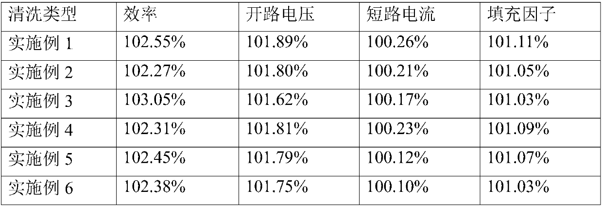
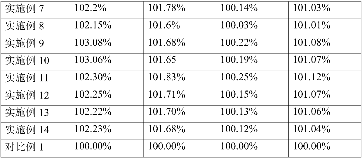
[0047] (1) Put the silicon chip into the first solution whose temperature is 60°C, and pass ozone into the first solution so that the ozone concentration in the first solution is 100 mg / liter, and the silicon The cleaning time of the tablet in the first solution is 8 minutes; wherein, the first solution includes hydrochloric acid, the volume ratio of the hydrochloric acid to the solute (ie water) is 1:6, and the mass fraction of the hydrochloric acid is 36%.
[0048] (2) The silicon chip is taken out from the first solution and put into a second solution, and the cleaning time of the silicon chip in the second solution is 3 minutes; wherein, the second solution includes hydrofluoric acid and Nitric acid, the volume ratio of the hydrofluoric acid to the nitric acid is 1:100, the mass fraction of the hydrofluoric acid is 49%, and the mass fraction of the nitric acid is 68%.
[0049] (3) Take the silicon chip out from the second solution, put it into a third solution with a tempe...
Embodiment 2
[0054] (1) Put the silicon chip into the first solution with a temperature of 58°C, and pass ozone into the first solution so that the ozone concentration in the first solution is 20 mg / liter, and the silicon The cleaning time of the sheet in the first solution is 9 minutes; wherein, the first solution includes hydrochloric acid and hydrogen peroxide, and the volume ratio of the hydrochloric acid, hydrogen peroxide and solute (i.e. water) is 1:2:7, and the hydrochloric acid Mass fraction is 20%, and the mass fraction of described hydrogen peroxide is 20%.
[0055] (2) The silicon chip is taken out from the first solution and put into a second solution, and the cleaning time of the silicon chip in the second solution is 4 minutes; wherein, the second solution includes hydrofluoric acid and Nitric acid, the volume ratio of the hydrofluoric acid to the nitric acid is 0.1:100, the mass fraction of the hydrofluoric acid is 30%, and the mass fraction of the nitric acid is 40%.
[0...
Embodiment 3
[0061] (1) Put the silicon chip into the first solution with a temperature of 70°C, and pass ozone into the first solution so that the ozone concentration in the first solution is 200 mg / liter, and the silicon The cleaning time of sheet in the first solution is 15 minutes; Wherein, described first solution comprises hydrochloric acid and hydrogen peroxide, and the volume ratio of described hydrochloric acid, hydrogen peroxide and solute (ie water) is 1:2:7, and the volume ratio of described hydrochloric acid Mass fraction is 45%, and the mass fraction of described hydrogen peroxide is 40%.
[0062] (2) The silicon chip is taken out from the first solution and put into a second solution, and the cleaning time of the silicon chip in the second solution is 5 minutes; wherein, the second solution includes hydrofluoric acid and Nitric acid, the volume ratio of the hydrofluoric acid to the nitric acid is 2:100, the mass fraction of the hydrofluoric acid is 70%, and the mass fraction...
PUM
| Property | Measurement | Unit |
|---|---|---|
| concentration | aaaaa | aaaaa |
Abstract
Description
Claims
Application Information
 - R&D
- Intellectual Property
- Life Sciences
- Materials
- Tech Scout
- Unparalleled Data Quality
- Higher Quality Content
- 60% Fewer Hallucinations
Browse by: Latest US Patents, China's latest patents, Technical Efficacy Thesaurus, Application Domain, Technology Topic, Popular Technical Reports.
© 2025 PatSnap. All rights reserved.Legal|Privacy policy|Modern Slavery Act Transparency Statement|Sitemap|About US| Contact US: help@patsnap.com


