
Patsnap Eureka
For R&D, Patsnap Eureka makes reading and utilizing patents & technical documents easy.
Patsnap Eureka AIR
Designed for self-driven R&D workflows. Generate viable solutions, solve complex R&D challenges, empower your innovation with AI.

Patsnap Eureka Materials
Designed for material experts only. Revolutionize your material R&D, from search, analyze, to developing new materials.

TechResearch
Generate reliable direction feasibility study reports for your R&D in just a few steps.

TechSeek
Discover and master advanced knowledge NOW. Basics, ideas, possibilities, all at once.

TechMind
As an expert in R&D Theories, TechMind can generates customized viable solutions instantly.

TechRisk
Analyze your overall solution with one click, know your potential R&D risks in advance.

TechMonitor
Get weekly tech updates, stay abreast of the latest tech innovations and key insights.
Silicon carbide epitaxial gallium oxide film method and silicon carbide epitaxial gallium oxide film structure
A thin-film structure and silicon carbide technology, applied in the field of microelectronics, can solve the problems of limited application, lattice mismatch, and limited application of power electronic devices, and achieve the effect of reducing dislocation defects and improving crystallinity
- Summary
- Abstract
- Description
- Claims
- Application Information
AI Technical Summary
Problems solved by technology
Method used
Image

Examples
Embodiment 1
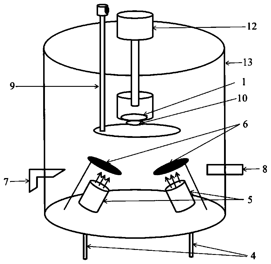
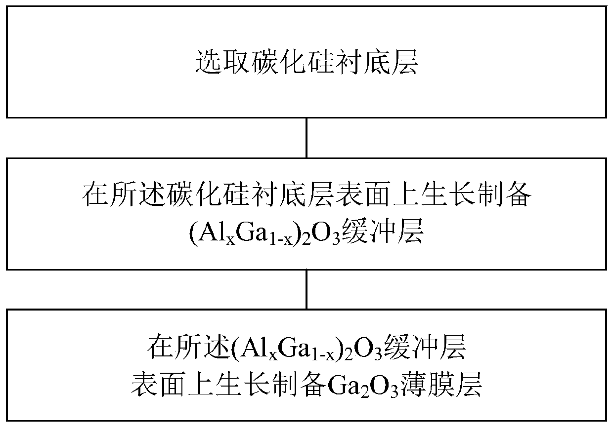
[0040] Before introducing the silicon carbide epitaxial gallium oxide thin film method provided in this embodiment, this embodiment first provides a device for preparing silicon carbide epitaxial gallium oxide thin film, please refer to figure 1 , figure 1 It is a schematic structural diagram of an equipment for preparing silicon carbide epitaxial gallium oxide thin films provided by an embodiment of the present invention. Pipeline 8 , substrate baffle 9 , tray 10 , substrate heating plate 11 , spinner 12 and sputtering chamber 13 . The radio frequency power supply 4 is connected to the target container 5 through the sputtering chamber 13 to provide power for the sputtering target. The target container 5 is used to place the sputtering target, and the two target baffles 6 are respectively arranged above the two target containers 5 . The gas inlet 7 can be provided with a plurality of gas pipes, and different gases can be fed in respectively. In this embodiment, the gas inlet...
Embodiment 2
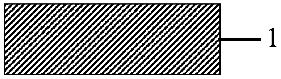
[0065] See Figure 5 , Figure 5 It is a schematic diagram of a silicon carbide epitaxial gallium oxide thin film structure provided by an embodiment of the present invention. An embodiment of the present invention provides a silicon carbide epitaxial gallium oxide thin film structure, the silicon carbide epitaxial gallium oxide thin film structure comprising: a silicon carbide substrate layer 1, (Al x Ga 1-x ) 2 o 3 buffer layer 2 and Ga 2 o 3 Thin film layer 3, wherein, (Al x Ga 1-x ) 2 o 3 The buffer layer 2 is located on the surface of the silicon carbide substrate layer 1, Ga 2 o 3 Thin film layer 3 is located at (Al x Ga 1-x ) 2 o 3 on the surface of the buffer layer 2.
[0066] The silicon carbide epitaxial gallium oxide thin film structure of this embodiment is prepared by using the silicon carbide epitaxial gallium oxide thin film method provided in the above embodiment, and its realization principle and technical effect are similar, and will not be re...
PUM
| Property | Measurement | Unit |
|---|---|---|
| Thickness | aaaaa | aaaaa |
| Thickness | aaaaa | aaaaa |
Abstract
Description
Claims
Application Information
 - R&D Engineer
- R&D Manager
- IP Professional
- Industry Leading Data Capabilities
- Powerful AI technology
- Patent DNA Extraction
Browse by: Latest US Patents, China's latest patents, Technical Efficacy Thesaurus, Application Domain, Technology Topic, Popular Technical Reports.
© 2024 PatSnap. All rights reserved.Legal|Privacy policy|Modern Slavery Act Transparency Statement|Sitemap|About US| Contact US: help@patsnap.com