Composite stacked lcp substrate and preparation method
A composite and substrate technology, applied in the direction of circuit substrate materials, printed circuits, printed circuit components, etc., to achieve the effects of low thermal expansion coefficient, good bonding strength and mechanical properties, and low Dk/Df
- Summary
- Abstract
- Description
- Claims
- Application Information
AI Technical Summary
Problems solved by technology
Method used
Image
Examples
Embodiment approach
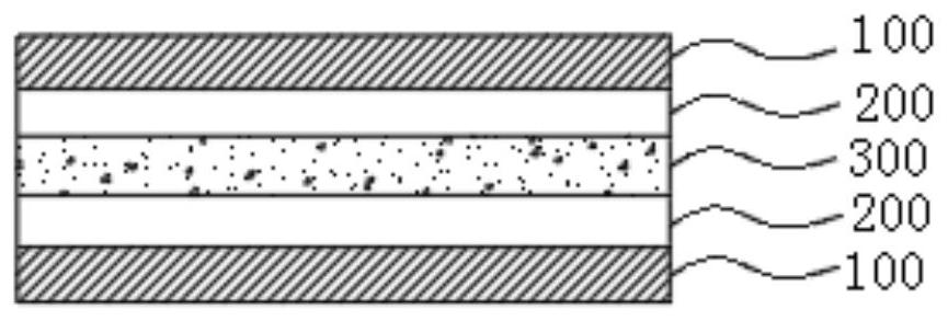
[0043] Implementation mode: a composite laminated LCP substrate, such as Figure 1 to Figure 2 As shown, it includes at least one copper foil layer 100, two low powder LCP layers 200, and a high powder LCP layer 300. The high powder LCP layer is located between the two low powder LCP layers. The copper foil The layer and the high-powder LCP layer are bonded by the low-powder LCP layer, and the content of the filler powder in the high-powder LCP layer is greater than that of the filler powder in the low-powder LCP layer Content, the low-powder LCP layer and the high-powder LCP layer both refer to LCP layers with a Dk value of 2.5-4.0 (10GHz) and a Df value of 0.001-0.005 (10GHz);
[0044] The thickness of each copper foil layer is 1-35 μm; the thickness of each low-powder LCP is 12-100 μm; the thickness of the high-powder LCP layer is 12-100 μm.
[0045] The low-powder LCP layer includes LCP and filler powder, the LCP is 70-100% (weight percentage) of the total solid content of the...
Embodiment approach 1
[0051] Embodiment 1: A composite laminated LCP substrate, such as figure 1 As shown, the LCP substrate is an LCP single-sided copper foil substrate, and the LCP single-sided copper foil substrate is composed of a copper foil layer 100, two low-powder LCP layers 200, and a high-powder LCP layer 300. The bottom is the copper foil layer 100, the low powder LCP layer 200, the high powder LCP layer 300, and the low powder LCP layer 200; the thickness of the LCP single-sided copper foil substrate is 37 -335μm.
[0052] The preparation method of the LCP single-sided copper foil substrate of Embodiment 1 is as follows:
[0053] Step 1: Coating the precursor of the low-powder LCP layer on one side of the copper foil layer, and removing the solvent at 60-180°C;
[0054] Step 2: Coating the precursor of the high-powder LCP layer on the lower surface of the low-powder LCP layer, and removing the solvent at 60-180°C;
[0055] Step 3. Coat the precursor of the low-powder LCP layer on the lower sur...
Embodiment approach 2
[0056] Embodiment 2: A composite laminated LCP substrate, such as figure 2 As shown, the LCP substrate is an LCP double-sided copper foil substrate. The LCP double-sided copper foil substrate is composed of two copper foil layers 100, two low-powder LCP layers 200, and a high-powder LCP layer 300. The bottom is the copper foil layer 100, the low powder LCP layer 200, the high powder LCP layer 300, the low powder LCP layer 200, and the copper foil layer 100; the LCP double-sided The thickness of the copper foil substrate is 38-370μm.
[0057] The preparation method of the LCP double-sided copper foil substrate of Embodiment 2 is one of the following two methods:
[0058] The first method includes the following steps:
[0059] Step 1. Coat the precursor of the low-powder LCP layer on one side of the copper foil layer, and remove the solvent at 60-180°C;
[0060] Step 2: Coating the precursor of the high-powder LCP layer on the lower surface of the low-powder LCP layer, and removing th...
PUM
| Property | Measurement | Unit |
|---|---|---|
| thickness | aaaaa | aaaaa |
| thickness | aaaaa | aaaaa |
| thickness | aaaaa | aaaaa |
Abstract
Description
Claims
Application Information
 - R&D Engineer
- R&D Manager
- IP Professional
- Industry Leading Data Capabilities
- Powerful AI technology
- Patent DNA Extraction
Browse by: Latest US Patents, China's latest patents, Technical Efficacy Thesaurus, Application Domain, Technology Topic, Popular Technical Reports.
© 2024 PatSnap. All rights reserved.Legal|Privacy policy|Modern Slavery Act Transparency Statement|Sitemap|About US| Contact US: help@patsnap.com


