Processing method for counterbore type PCB

A technology of PCB board and processing method is applied in the processing field of countersunk hole type PCB board, which can solve the problems of increasing the assembly volume of the whole machine and reducing the thickness, and achieves the effect of small assembly volume and smooth installation of the whole machine.

Pending Publication Date: 2020-02-25
星河电路(福建)有限公司
View PDF5 Cites 3 Cited by
  • Summary
  • Abstract
  • Description
  • Claims
  • Application Information

AI Technical Summary

Problems solved by technology

[0003] In the process of designing and manufacturing conventional printed circuit boards, in order to achieve and cooperate with the overall volume of the client, the product stack structure and wiring density are generally increased to reduce the overall thickness of the circuit board as much as possible, but limited by the wiring lines. Wide line spacing and multi-layer process processing capability, in the design and manufacturing process, the thickness reduction is limited
[0004] Under normal circumstances, after the printed circuit board is shipped to the client, electronic components must be assembled. Electronic components are generally attached to the surface of the circuit board, so they will form protrusions and increase the assembly volume of the whole machine. Therefore, how to improve the circuit board The structure to make it more flat has become an urgent technical problem in the field of PCB board processing

Method used


Image

  • Processing method for counterbore type PCB

Examples


Embodiment Construction

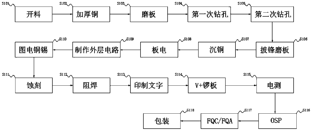
[0024] Those skilled in the art understand that, as mentioned in the background art, when the PCB board in the prior art is assembled with electronic components, it will form protrusions and increase the assembly volume of the whole machine. Therefore, it is necessary to improve the structure of the circuit board so that it tends to Yu flat.

[0025] To this end, an embodiment of the present invention provides a method for processing a counterbore PCB board, including:

[0026] Thicken the copper, thicken the copper on the PCB board, and increase the thickness of the copper foil on the PCB;

[0027] For the first drilling, the circular drill bit is used to drill the thickened copper-treated PCB board, and the conduction holes and positioning holes are processed;

[0028] For the second drilling, the taper drill is used for secondary processing, and the countersink is processed;

[0029] Etching, using the step-by-step etching method, etch the front and back of the drilled PC...


PUM


Abstract

The invention discloses a processing method for a counterbore type PCB, which relates to the technical field of electronic processing. The method comprises the following steps of: thickening copper, and thickening copper on the PCB to increase the thickness of copper foil on the PCB, drilling for the first time, drilling the PCB subjected to the copper thickening treatment by adopting a circular drill bit and processing a via hole and a positioning hole, conducting secondary drilling, adopting a conical drill bit for secondary machining, and processing a counterbore, etching, etching the frontsurface and the back surface of the drilled PCB in sequence by adopting a fractional etching method, and resistance welding: carrying out twice resistance welding screen printing on the etched PCB byadopting a Line Mask film alignment exposure method. Firstly, copper thickening treatment is carried out on a PCB, and then counterbores are formed through two times of drilling. Due to the design ofthe counterbores of the PCB, the overall assembly size of the electronic product is small, and the assembly is smoother during installation.

Description

technical field [0001] The invention relates to the technical field of electronic processing, in particular to a method for processing counterbore-type PCB boards. Background technique [0002] With the development of electronic products in the direction of lightness, thinness, shortness and smallness, the volume, appearance and installation of the printed circuit board must be considered in the process of assembling electronic components and designing the whole machine on the client side. Flatness, which forces printed circuit boards to develop towards higher precision wiring, stacking and special process design. [0003] In the process of designing and manufacturing conventional printed circuit boards, in order to achieve and cooperate with the overall volume of the client, the product stack structure and wiring density are generally increased to reduce the overall thickness of the circuit board as much as possible, but limited by the wiring lines. Wide line spacing and m...

Claims


Application Information

Patent Timeline
Patent Type & Authority Applications(China)
IPC IPC(8): H05K3/18H05K3/00H05K3/28
CPCH05K3/18H05K3/0047H05K3/28
Inventor 陈玲黄江波张军
Owner 星河电路(福建)有限公司
Why Eureka
Try Eureka