Pixel structure

A pixel structure, thin film transistor technology, applied in optics, instruments, electrical components, etc., can solve problems such as drop

Active Publication Date: 2020-02-21
AU OPTRONICS CORP
View PDF5 Cites 2 Cited by
  • Summary
  • Abstract
  • Description
  • Claims
  • Application Information

AI Technical Summary

Problems solved by technology

In a lighting environment, when the display panel is used, part of the signal line and / or active components will reflect the ambient light beam, resulting in a decrease in the ambient contrast (Ambient Contrast Ratio; ACR) of the display panel

Method used


Image

  • Pixel structure
  • Pixel structure
  • Pixel structure

Examples


Embodiment Construction

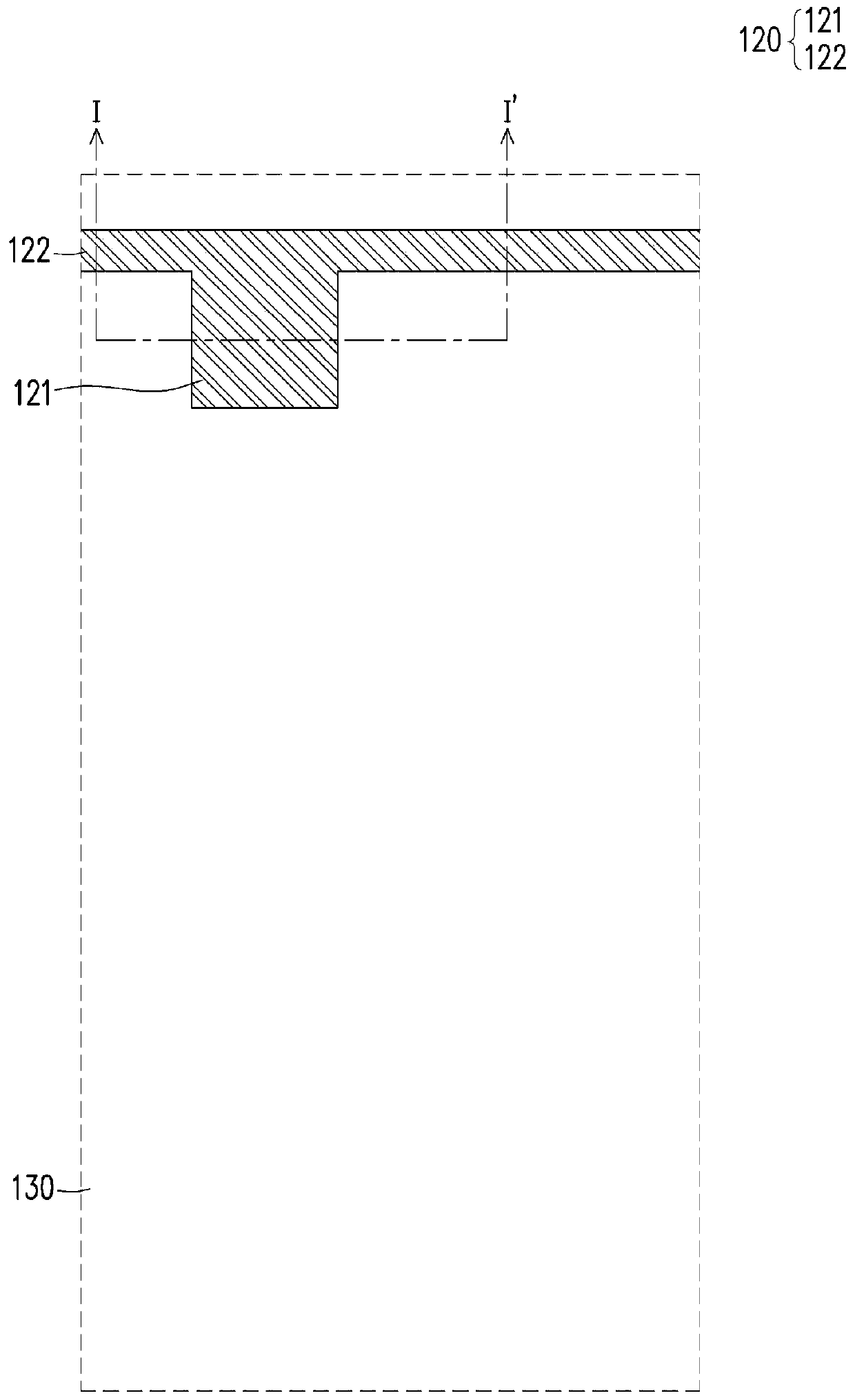
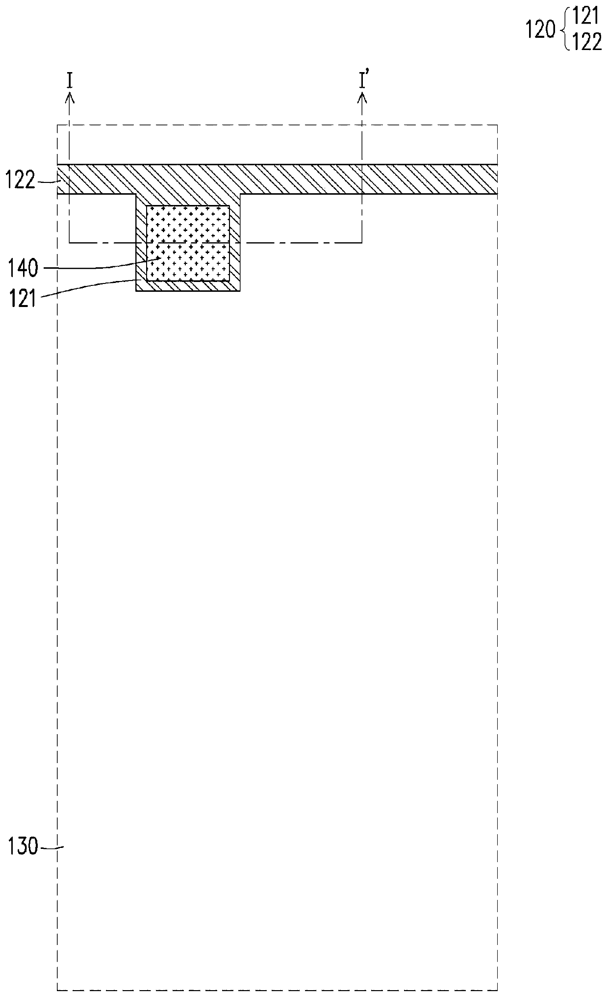
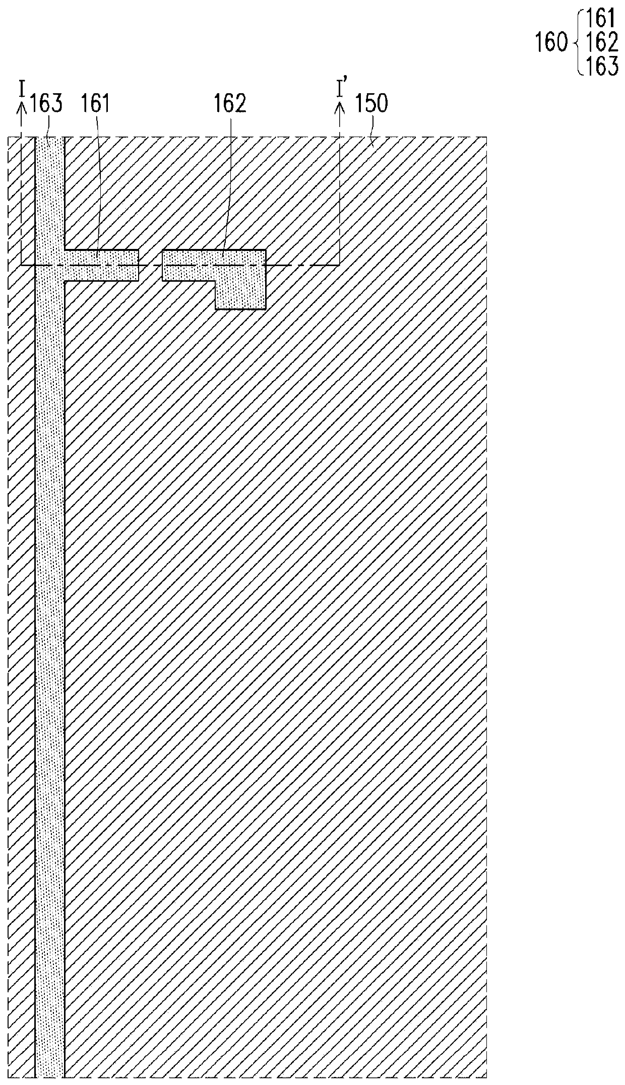
[0050] Reference will now be made in detail to the exemplary embodiments of the present invention, examples of which are illustrated in the accompanying drawings. Wherever possible, the same reference numbers will be used in the drawings and description to refer to the same or like parts.

[0051] It will be understood that when an element such as a layer, film, region, or substrate is referred to as being "on" or "connected to" another element, it can be directly on or connected to the other element, or Intermediate elements may also be present. In contrast, when an element is referred to as being "directly on" or "directly connected to" another element, there are no intervening elements present. As used herein, "connected" may refer to physical and / or electrical connection. Furthermore, "electrically connected" or "coupled" may mean that other elements exist between two elements.

[0052] As used herein, "about," "approximately," or "substantially" includes stated values ...


PUM


Abstract

A pixel structure comprises a substrate, a thin film transistor arranged on the substrate and provided with a first end, a second end and a control end, a first signal line electrically connected to the first end of the thin film transistor, a second signal line electrically connected to the control end of the thin film transistor, a pixel electrode electrically connected to the second end of thethin film transistor and a shading layer. At least one of the first end of the thin film transistor, the second end of the thin film transistor, the control end of the thin film transistor, the firstsignal line and the second signal line is formed by a conductive layer. The shading layer is arranged on the top surface and the side wall of the conducting layer. The light shielding layer comprisesphotoresist and a plurality of particles mixed with the photoresist.

Description

technical field [0001] The invention relates to a pixel structure. Background technique [0002] The display panel includes a pixel array substrate, an opposite substrate, and a display medium arranged between the pixel array substrate and the opposite substrate. The pixel array substrate includes a substrate and a plurality of pixel structures arranged on the substrate. Each pixel structure includes a signal line, an active element electrically connected to the signal line, and a pixel electrode electrically connected to the active element. [0003] Generally speaking, due to the consideration of electrical conductivity, signal lines and / or a part of active components are usually made of metal layers. The metal layer is very conductive, but it is reflective. In a lighting environment, when the display panel is used, a part of the signal line and / or the active element will reflect the ambient light, causing the Ambient Contrast Ratio (ACR) of the display panel to decrease...

Claims


Application Information

Patent Timeline
Patent Type & Authority Applications(China)
IPC IPC(8): H01L27/12
CPCH01L27/1214H01L27/124G02F1/0063H10K59/1213H10K50/865H10K59/123H10K59/126
Inventor 杜振源吴振中林岱佐
Owner AU OPTRONICS CORP
Why Eureka
Try Eureka