Power supply selection module for sight and solar sight with same
A power supply selection and light source module technology, applied in the field of solar sights, can solve the problems of battery power consumption, processing chip consumption control power consumption, and inability to effectively prolong battery life and battery life, so as to save power and prolong life and the effect of battery life
- Summary
- Abstract
- Description
- Claims
- Application Information
AI Technical Summary
Problems solved by technology
Method used
Image
Examples
Embodiment 1
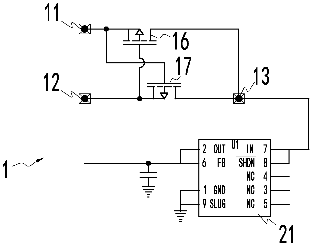
[0038] Embodiment 1: as figure 1 As shown, the first voltage-controlled switch 14 and the second voltage-controlled switch 15 in the power selection module 1 are respectively the first PMOS transistor 16 and the second PMOS transistor 17, and the first power input terminal 11 and the second The two power supply input terminals 12 are respectively connected to the input terminal of the first PMOS transistor 16 and the input terminal of the second PMOS transistor 17, and the output terminal of the first PMOS transistor 16 is connected to the output of the second PMOS transistor 17. terminal is connected to the power output terminal 13, the control terminal of the first PMOS transistor 16 is connected to the second power input terminal 12, and the control terminal of the second PMOS transistor 17 is connected to the first power input terminal 11 connect. It should be noted that both the first PMOS transistor 16 and the second PMOS transistor are P-channel field effect transistor...
Embodiment 2
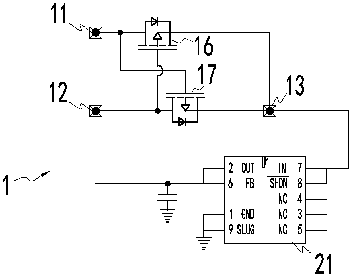
[0042] Embodiment 2: as figure 2 As shown, the difference from Embodiment 1 is that both the first PMOS transistor 16 and the second PMOS transistor 17 have parasitic diodes, and the first power input terminal 11 and the second power input terminal 12 are connected to the first PMOS transistor 16 respectively. The drain is connected to the drain of the second PMOS transistor 17 , and the source of the first PMOS transistor 16 and the source of the second PMOS transistor 17 are connected to the power output terminal 13 in parallel. Same as Embodiment 1, the gate of the first PMOS transistor 16 is connected to the second power input terminal 12 , and the gate of the second PMOS transistor 17 is connected to the first power input terminal 11 . from figure 2 It can be known from the connection method shown that the Ugs of the first PMOS transistor 16 refers to the potential difference between the second power input terminal 12 and the power output terminal 13, and the Ugs of th...
Embodiment 3
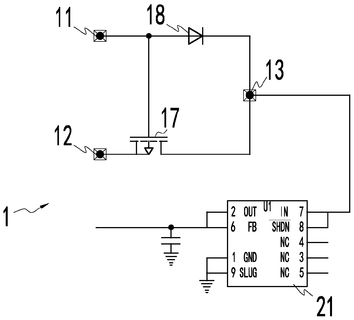
[0043] Embodiment 3: as image 3As shown, the difference from Embodiment 1 is that the first PMOS transistor 16 is replaced by a first one-way diode 18, and the first power supply input terminal 11 is placed at the anode of the first one-way diode 18, so The cathode of the first unidirectional diode 18 is connected to the output terminal 13 of the power supply. When the potential of the first power input terminal 11 is lower than the potential of the second power input terminal 12, the second PMOS transistor 17 is turned on, and at this time the first unidirectional diode 18 is in a reverse biased state, and the current can only pass through the second PMOS. The tube 17 flows to the power output terminal 13; when the potential of the first power input terminal 11 is greater than the potential of the second power input terminal 12, the second PMOS tube 17 is cut off, and at this time the first unidirectional diode 18 is in a forward biased state, Current can only flow to the p...
PUM
 Abstract
Description
Claims
Application Information
 - R&D
- Intellectual Property
- Life Sciences
- Materials
- Tech Scout
- Unparalleled Data Quality
- Higher Quality Content
- 60% Fewer Hallucinations
Browse by: Latest US Patents, China's latest patents, Technical Efficacy Thesaurus, Application Domain, Technology Topic, Popular Technical Reports.
© 2025 PatSnap. All rights reserved.Legal|Privacy policy|Modern Slavery Act Transparency Statement|Sitemap|About US| Contact US: help@patsnap.com


