Manufacturing method of SOI

A manufacturing method and technology of silicon wafers, applied in semiconductor/solid-state device manufacturing, electrical components, circuits, etc., can solve problems such as poor bonding force at the edge of the bonding surface, tearing or cracking of the edge of the silicon wafer, and reduced SOI yield , to increase the bonding force, avoid tearing or cracking, and reduce the number of waste products

Pending Publication Date: 2020-01-31
SHENYANG SILICON TECH
View PDF0 Cites 0 Cited by
  • Summary
  • Abstract
  • Description
  • Claims
  • Application Information

AI Technical Summary

Problems solved by technology

[0003] In the related art, when manufacturing SOI (Silicon-On-Insulator, silicon on an insulating substrate), it is usually realized by bonding, that is, an oxide layer is formed on at least one of the two silicon wafers, and at room temperature The two silicon wafers are bonded together to form a bonded body. However, due to the poor bonding force at the edge of the bonding surface, it is easy to cause the edge of the silicon wafer to tear or crack during the subsequent process, and even lead to the scrapping of the SOI, which reduces the finished product of the SOI. Rate

Method used


Image

  • Manufacturing method of SOI
  • Manufacturing method of SOI
  • Manufacturing method of SOI

Examples


Embodiment Construction

[0024] In order to understand the above-mentioned purpose, features and advantages of the present invention more clearly, the present invention will be further described in detail below in conjunction with the accompanying drawings and specific embodiments. It should be noted that, in the case of no conflict, the embodiments of the present application and the features in the embodiments can be combined with each other.

[0025] In the following description, many specific details are set forth in order to fully understand the present invention. However, the present invention can also be implemented in other ways different from those described here. Therefore, the protection scope of the present invention is not limited by the specific details disclosed below. EXAMPLE LIMITATIONS.

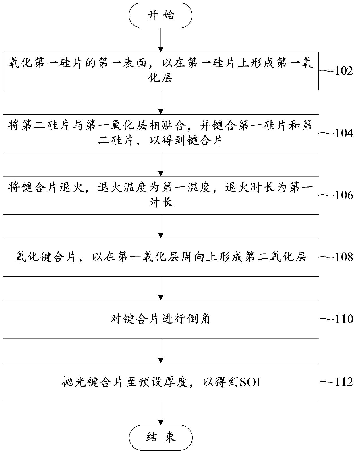
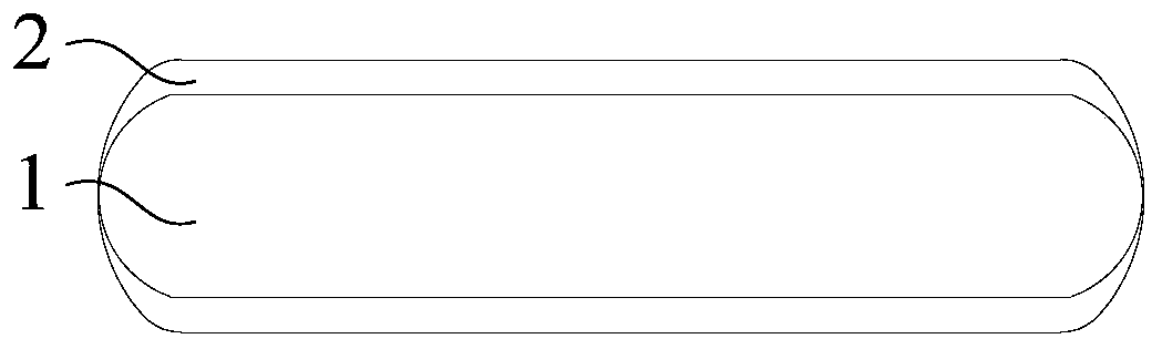
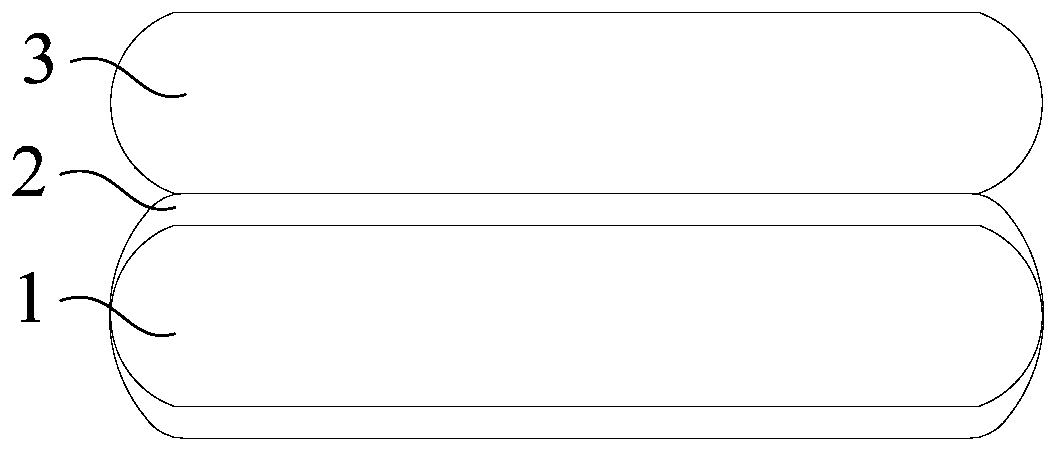
[0026] Refer below Figure 1 to Figure 6 A method of manufacturing the SOI according to some embodiments of the present invention is described.

[0027] In the embodiment of the first aspect of the...


PUM

PropertyMeasurementUnit
widthaaaaaaaaaa

Abstract

The invention provides a manufacturing method of SOI. The manufacturing method comprises the following steps: oxidizing the first surface of a first silicon wafer to form a first oxide layer on the first silicon wafer; bonding the second silicon wafer with the first oxide layer and bonding the first silicon wafer and the second silicon wafer so as to obtain a bonding wafer; annealing the bonding wafer, wherein the annealing temperature is the first temperature and the annealing time is the first time; oxidizing the bonding wafer to form a second oxide layer in the circumferential direction ofthe first oxide layer; and chamfering he oxidized bonding wafer and polishing the boding wafer to the preset thickness so as to obtain the SOI. According to the manufacturing method of the SOI, the second oxide layer is formed around the first oxide layer so that the unbonded part between the first silicon wafer and the second silicon wafer is filled by the second oxide layer, the bonding force between the first silicon wafer and the second silicon wafer is increased, the edge of the bonding wafer is prevented from tearing or cracking, the amount of waste products is reduced and the yield of the SOI is improved; and the force bearing of the polished surface is more uniform.

Description

technical field [0001] The present invention relates to the technical field of SOI, in particular, to a method for manufacturing SOI. Background technique [0002] At present, with the continuous development of silicon material processing technology, people have paid more and more attention to the processing quality of wafers. [0003] In the related art, when manufacturing SOI (Silicon-On-Insulator, silicon on an insulating substrate), it is usually realized by bonding, that is, an oxide layer is formed on at least one of the two silicon wafers, and at room temperature The two silicon wafers are bonded together to form a bonded body. However, due to the poor bonding force at the edge of the bonding surface, it is easy to cause the edge of the silicon wafer to tear or crack during the subsequent process, and even lead to the scrapping of the SOI, which reduces the finished product of the SOI. Rate. Contents of the invention [0004] The present invention aims to solve at...

Claims


Application Information

Patent Timeline
Patent Type & Authority Applications(China)
IPC IPC(8): H01L21/762
CPCH01L21/76251H01L21/76275
Inventor 彦丙智
Owner SHENYANG SILICON TECH
Why Eureka
Try Eureka