Silicon-based negative electrode active material and its preparation method and application
A technology of active materials and silicon-based negative electrodes, applied in nanotechnology for materials and surface science, battery electrodes, final product manufacturing, etc., can solve the problem of loss of electrical contact between electrode active materials and current collectors, hindering the practical application of silicon negative electrode materials , reduce battery rate performance and other issues, to achieve the effect of large-scale industrial production, simple and efficient preparation method, and excellent rate performance
- Summary
- Abstract
- Description
- Claims
- Application Information
AI Technical Summary
Problems solved by technology
Method used
Image
Examples
preparation example Construction
[0054] The present invention also provides a method for preparing a silicon-based negative electrode active material, the method comprising:
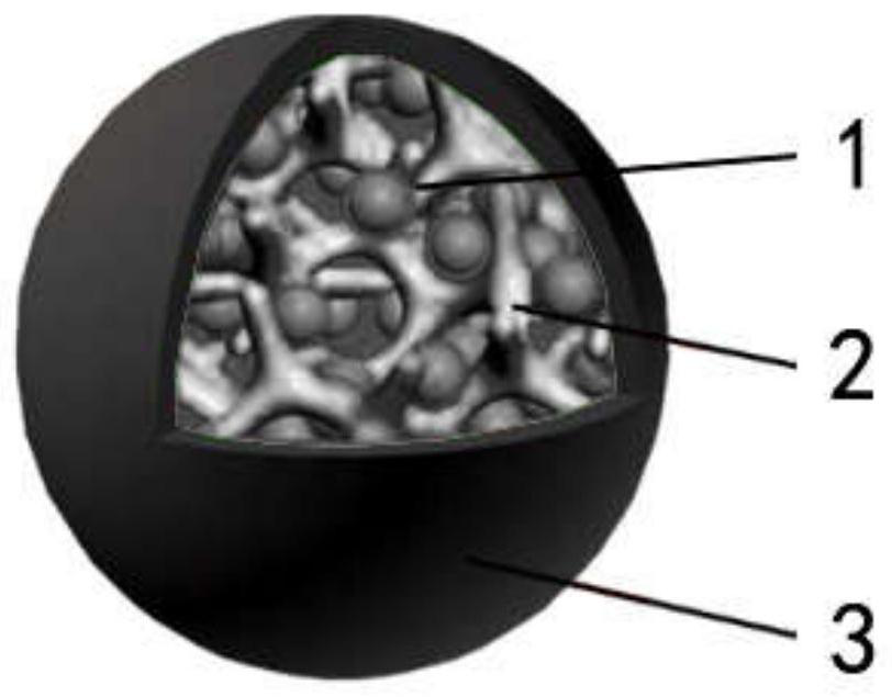
[0055] (1) In situ polymerizing aniline monomers on the surface of silicon nanoparticles to form a polyaniline crosslinked three-dimensional network structure to obtain a silicon / polyaniline composite material;
[0056] (2) molding the silicon / polyaniline composite material;
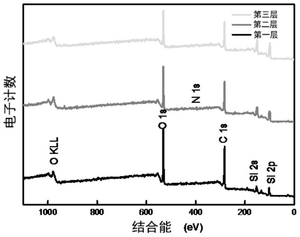
[0057] (3) Convert at least part of the surface layer of the formed silicon / polyaniline composite material into a carbonized layer by carbonization treatment.
[0058] According to the present invention, the particle size of the silicon nanoparticles is not particularly limited, for example, it may be 500 nm or less. From the perspective of facilitating the transport of lithium ions and suppressing the volume effect of the material, the particle size of the silicon nanoparticles is preferably within 300nm, more preferably within 200nm, for example, it can be 20-2...
Embodiment 1
[0076] (1) In-situ polymerization: 1.273g phytic acid, 0.419g aniline monomer and 4g silicon nanoparticles (particle size: 100nm) were mixed and recorded as solution A; 0.428g ammonium persulfate was dissolved in 15mL deionized water and recorded as Solution B: Mix solution A and solution B, stir (20h) and sonicate (100Hz, 30min) to obtain a silicon / polyaniline composite material with a three-dimensional porous network structure.
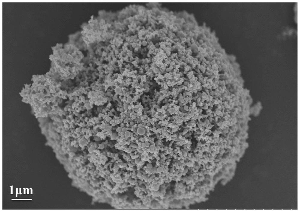
[0077] (2) Spray drying: the silicon / polyaniline composite material in step (1) is spray-dried to obtain silicon / polyaniline microspheres (average particle diameter is 10 μm), wherein the spray drying conditions include: air inlet temperature 180 ℃, air outlet temperature 60 ℃, peristaltic pump rate 8%, needle pass frequency 2 times per second.
[0078] (3) Surface carbonization: heat the silicon / polyaniline microspheres in step (2) at a temperature of 500° C. for 1 hour in a tube furnace fed with argon, and heat up at a rate of 5° C. / min to make th...
preparation example 1
[0088] The silicon-based negative electrode active materials of the above-mentioned examples and comparative examples were ground and evenly coated with conductive carbon black (Super P), sodium carboxymethylcellulose, and styrene-butadiene latex according to a weight ratio of 8:1:0.5:0.5. Copper foil current collector, and vacuum drying at 120 ° C to obtain a negative electrode sheet.
PUM
| Property | Measurement | Unit |
|---|---|---|
| particle diameter | aaaaa | aaaaa |
| particle diameter | aaaaa | aaaaa |
| particle diameter | aaaaa | aaaaa |
Abstract
Description
Claims
Application Information
 - R&D
- Intellectual Property
- Life Sciences
- Materials
- Tech Scout
- Unparalleled Data Quality
- Higher Quality Content
- 60% Fewer Hallucinations
Browse by: Latest US Patents, China's latest patents, Technical Efficacy Thesaurus, Application Domain, Technology Topic, Popular Technical Reports.
© 2025 PatSnap. All rights reserved.Legal|Privacy policy|Modern Slavery Act Transparency Statement|Sitemap|About US| Contact US: help@patsnap.com


