Method for texturing silicon wafer by repeatedly utilizing nitrogen-free black silicon cleaning solution
A cleaning fluid, black silicon technology, applied in the direction of final product manufacturing, sustainable manufacturing/processing, electrical components, etc., can solve the problem of high cost, and achieve the effect of reducing the cost of texturing and wastewater treatment
- Summary
- Abstract
- Description
- Claims
- Application Information
AI Technical Summary
Problems solved by technology
Method used
Image
Examples
Embodiment 1
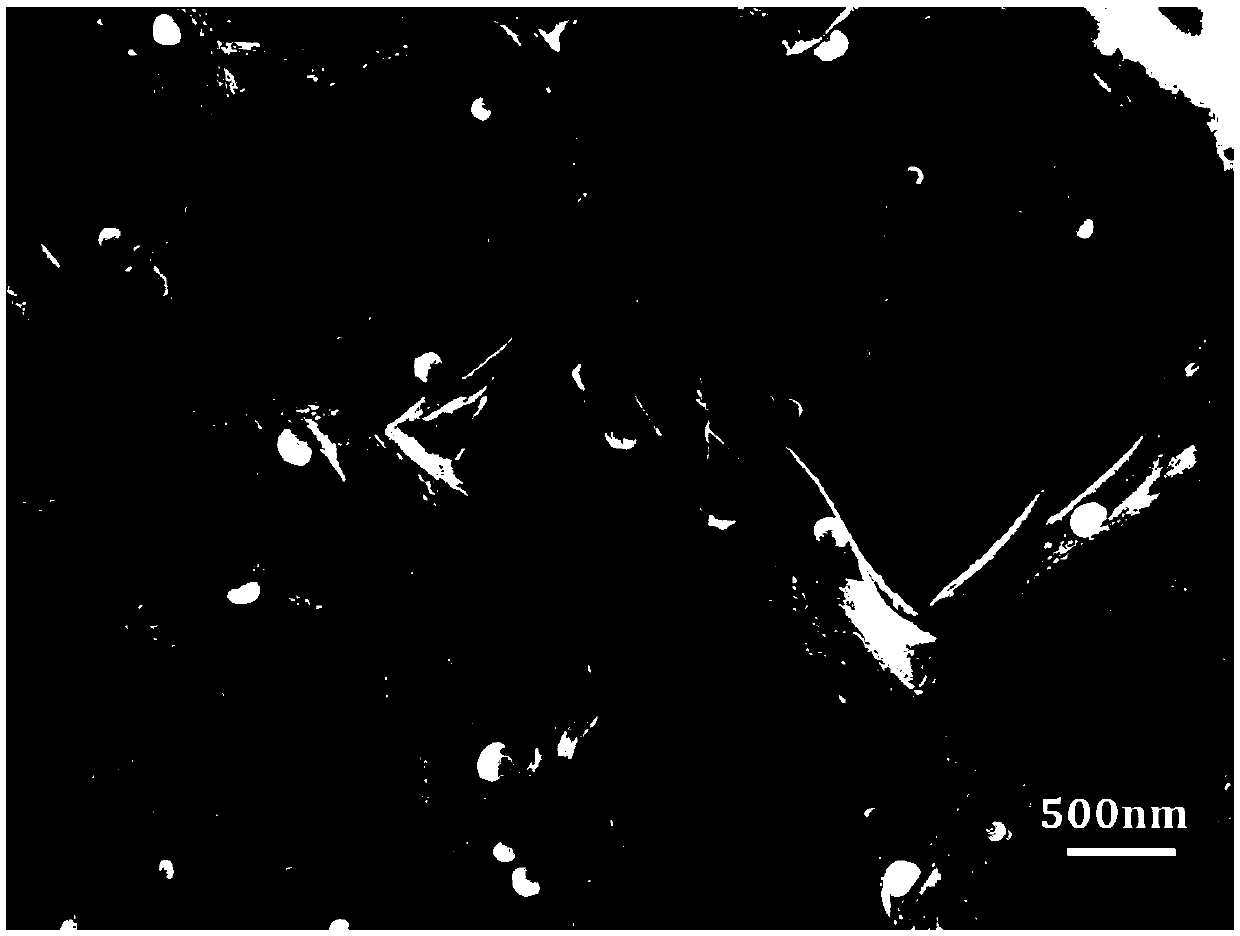
[0051] Step 1: Take a P-type diamond wire-cut monocrystalline silicon wafer with a size of 156mm×156mm (resistivity 1-3Ωcm), and immerse it in the acidic black silicon texturing solution in the texturing tank for texturing, and the reaction temperature is 45°C , the reaction time is 5 minutes, and discretely distributed copper metal particles are formed on the surface of the silicon wafer; among them, the acidic black silicon texturing solution is prepared from copper nitrate, hydrofluoric acid and hydrogen peroxide, the total volume is 200L, and the concentration of copper ions is 5mmol / L, the concentration of hydrofluoric acid is 4.5mol / L, and the concentration of hydrogen peroxide is 0.6mol / L.
[0052] Step 2: Take out the textured silicon wafer obtained in Step 1, wash it with deionized water, and dry it with high-purity nitrogen.
[0053] Step 3: Wash the dried silicon wafer obtained in Step 2 with a nitrogen-free black silicon cleaning solution for 3 minutes at 60°C to r...
Embodiment 2
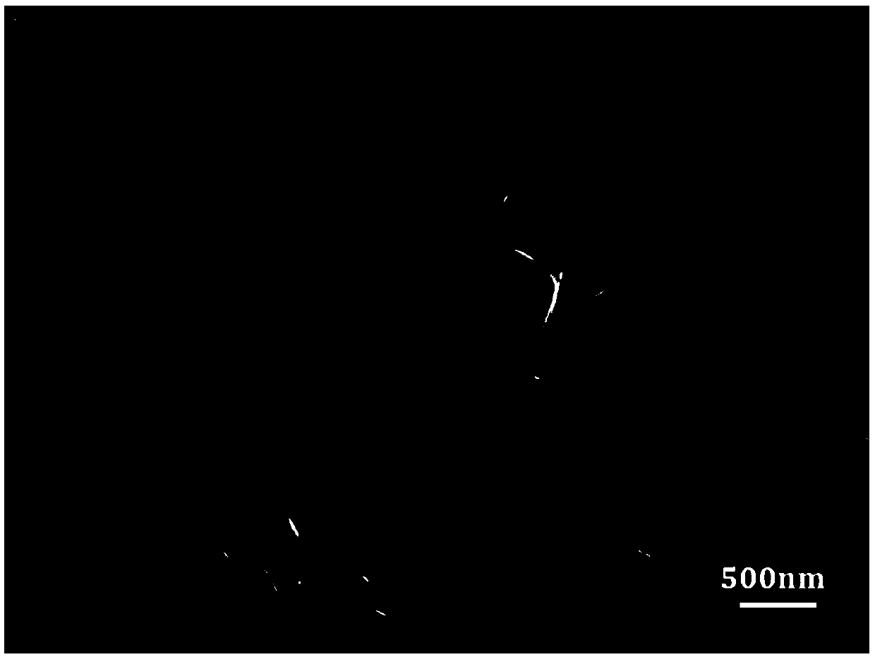
[0062] Step 1: Take a P-type diamond wire-cut polysilicon wafer (resistivity 1-3Ωcm) with a size of 156mm×156mm, and immerse it in the acidic black silicon texturing solution in the texturing tank for texturing. The reaction temperature is 50°C. The time is 3 minutes, and discretely distributed copper metal particles are formed on the surface of the silicon wafer; among them, the acidic black silicon texturing solution is prepared from copper nitrate, hydrofluoric acid and hydrogen peroxide, the total volume is 300L, and the concentration of copper ions is 2mmol / L, the concentration of hydrofluoric acid is 3mol / L, and the concentration of hydrogen peroxide is 2mol / L.
[0063] Step 2: Take out the textured silicon wafer obtained in Step 1, wash it with deionized water, and dry it with high-purity nitrogen.
[0064] Step 3: Wash the dried silicon wafer obtained in Step 2 with a nitrogen-free black silicon cleaning solution for 3 minutes at 50°C to remove copper metal particles ...
Embodiment 3
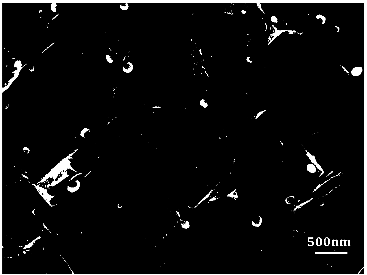
[0070] Step 1: Take a P-type diamond wire-cut polycrystalline silicon wafer (resistivity 1-3Ωcm) with a size of 156mm×156mm, and immerse it in the acidic black silicon texturing solution in the texturing tank for texturing. The reaction temperature is 40°C. The time is 4 minutes, and discretely distributed copper metal particles are formed on the surface of the silicon wafer; the acidic black silicon texturing solution is prepared from copper nitrate, hydrofluoric acid and hydrogen peroxide, the total volume is 200L, and the concentration of copper ions is 0.5mmol / L, the concentration of hydrofluoric acid is 6mol / L, and the concentration of hydrogen peroxide is 1.5mol / L.
[0071] Step 2: Take out the textured silicon wafer obtained in Step 1, wash it with deionized water, and dry it with high-purity nitrogen.
[0072] Step 3: Wash the dried silicon wafer obtained in Step 2 with a nitrogen-free black silicon cleaning solution for 3 minutes at 25°C to remove copper metal partic...
PUM
| Property | Measurement | Unit |
|---|---|---|
| Resistivity | aaaaa | aaaaa |
Abstract
Description
Claims
Application Information
 - R&D
- Intellectual Property
- Life Sciences
- Materials
- Tech Scout
- Unparalleled Data Quality
- Higher Quality Content
- 60% Fewer Hallucinations
Browse by: Latest US Patents, China's latest patents, Technical Efficacy Thesaurus, Application Domain, Technology Topic, Popular Technical Reports.
© 2025 PatSnap. All rights reserved.Legal|Privacy policy|Modern Slavery Act Transparency Statement|Sitemap|About US| Contact US: help@patsnap.com


