Array substrate, manufacturing method thereof and display panel

A technology of an array substrate and a manufacturing method, applied in the display field, can solve problems such as the reduction of pixel aperture ratio, and achieve the effects of increasing capacitance value, small capacitance area, and high resolution

Inactive Publication Date: 2020-01-17
SHENZHEN CHINA STAR OPTOELECTRONICS SEMICON DISPLAY TECH CO LTD
View PDF5 Cites 1 Cited by
  • Summary
  • Abstract
  • Description
  • Claims
  • Application Information

AI Technical Summary

Problems solved by technology

[0003] In large-size and high-resolution display panels, due to the relatively large proportion of thin film transistors and capacitor areas, and the structure of thin film transistors is opaque, the aperture ratio of pixels will be reduced. The current solution is to minimize the area of ​​thin film transistors and capacitors. , but capacitors and thin film transistors need a certain size to ensure the function, and the reduction is limited

Method used


Image

  • Array substrate, manufacturing method thereof and display panel
  • Array substrate, manufacturing method thereof and display panel
  • Array substrate, manufacturing method thereof and display panel

Examples


Embodiment Construction

[0050] The following descriptions of the various embodiments refer to the accompanying drawings to illustrate specific embodiments in which the invention may be practiced. The directional terms mentioned in the present invention, such as [top], [bottom], [front], [back], [left], [right], [inside], [outside], [side], etc., are only for reference The orientation of the attached schema. Therefore, the directional terms used are used to illustrate and understand the present invention, but not to limit the present invention. In the figures, structurally similar elements are denoted by the same reference numerals.

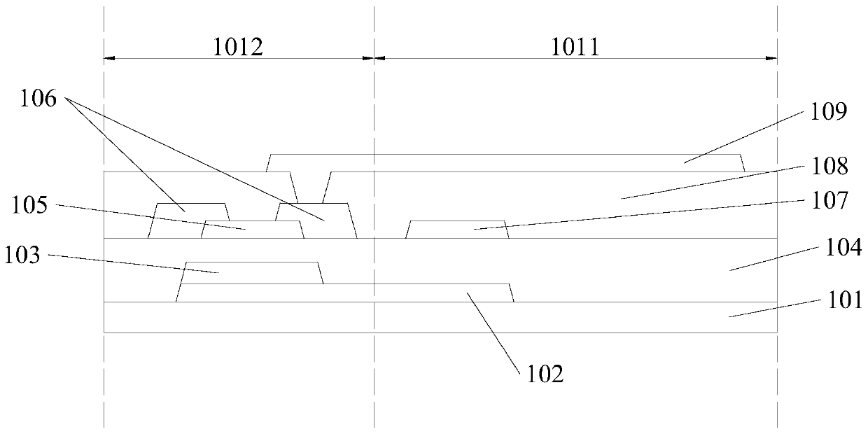
[0051] see figure 1 The existing array substrate is divided into a light-emitting area 1011 and a non-light-emitting area 1012. The array substrate includes: a base substrate 101, a first transparent electrode 102 disposed on the base substrate 101, a grid 103, a gate insulating layer 104, an Source layer 105, source drain 106, second transparent electrode 107, passiv...


PUM


Abstract

The invention provides an array substrate, a manufacturing method thereof and a display panel. The array substrate comprises a light-emitting area and a non-light-emitting area, and the array substrate comprises a substrate base plate; gate insulating layers which comprise a first gate insulating layer and a second gate insulating layer which are sequentially arranged on the substrate base plate;a storage capacitor which is located in the light-emitting area and comprises a first transparent electrode and a second transparent electrode, wherein the first transparent electrode is arranged between the first gate insulating layer and the second gate insulating layer, and the second transparent electrode is arranged on the second gate insulating layer and is opposite to the first transparentelectrode in position. According to the array substrate, the yield of products is increased, and the aperture opening ratio of pixels is increased. According to the display panel, the aperture openingratio of the pixels is large, and the resolution ratio during display is high.

Description

technical field [0001] The present invention relates to the field of display technology, in particular to an array substrate, a manufacturing method thereof, and a display panel. Background technique [0002] At present, both LCD (Liquid Crystal Display, liquid crystal display) and OLED (Organic Light-Emitting Diode, organic light-emitting diode) have their own advantages, and are widely used in display devices. Both LCD and OLED include array substrates. Each pixel is controlled by a thin film transistor (TFT). Wherein, a thin film transistor generally includes a gate, an active layer, a source, and a drain. Specifically, the structure of the thin film transistor may be a bottom gate type or a top gate type. [0003] In large-size and high-resolution display panels, due to the relatively large proportion of thin film transistors and capacitor areas, and the structure of thin film transistors is opaque, the aperture ratio of pixels will be reduced. The current solution is t...

Claims


Application Information

Patent Timeline
Patent Type & Authority Applications(China)
IPC IPC(8): H01L27/12H01L21/77
CPCH01L27/1255H01L27/1259H01L29/66969H01L29/7869H01L27/1225H01L27/124H01L27/1237H01L27/127H01L27/1288
Inventor 林振国周星宇徐源竣
Owner SHENZHEN CHINA STAR OPTOELECTRONICS SEMICON DISPLAY TECH CO LTD
Why Eureka
Try Eureka