PCB manufacturing method

A manufacturing method and film technology, applied in the directions of printed circuit manufacturing, multilayer circuit manufacturing, electrical components, etc., can solve the problems of unreachable, large signal loss, unfavorable signal transmission and reception, etc., to enhance the ability to resist external pressure, reduce Effects of Signal Transmission Loss

Active Publication Date: 2019-12-31
DONGGUAN SHENGYI ELECTRONICS
View PDF9 Cites 2 Cited by
  • Summary
  • Abstract
  • Description
  • Claims
  • Application Information

AI Technical Summary

Problems solved by technology

However, when the upper and lower layers of the inner layer are covered by a dielectric layer, the signal loss of the PCB produced by the existing technology is still very large, which cannot meet the requirements of wireless radio frequency products above 70 GHz, which is not conducive to signal transmission and reception.

Method used


Image

  • PCB manufacturing method
  • PCB manufacturing method
  • PCB manufacturing method

Examples


Embodiment Construction

[0035] In order to make the technical problems solved by the present invention, the technical solutions adopted and the technical effects achieved clearer, the technical solutions of the embodiments of the present invention will be further described in detail below in conjunction with the accompanying drawings. Obviously, the described embodiments are only the technical solutions of the present invention. Some, but not all, embodiments.

[0036] This embodiment provides a method for manufacturing a PCB, which is suitable for manufacturing a PCB with a high-frequency signal transmission line, and can form a cavity on one side of the high-frequency signal transmission line to reduce the loss of signal transmission in the medium.

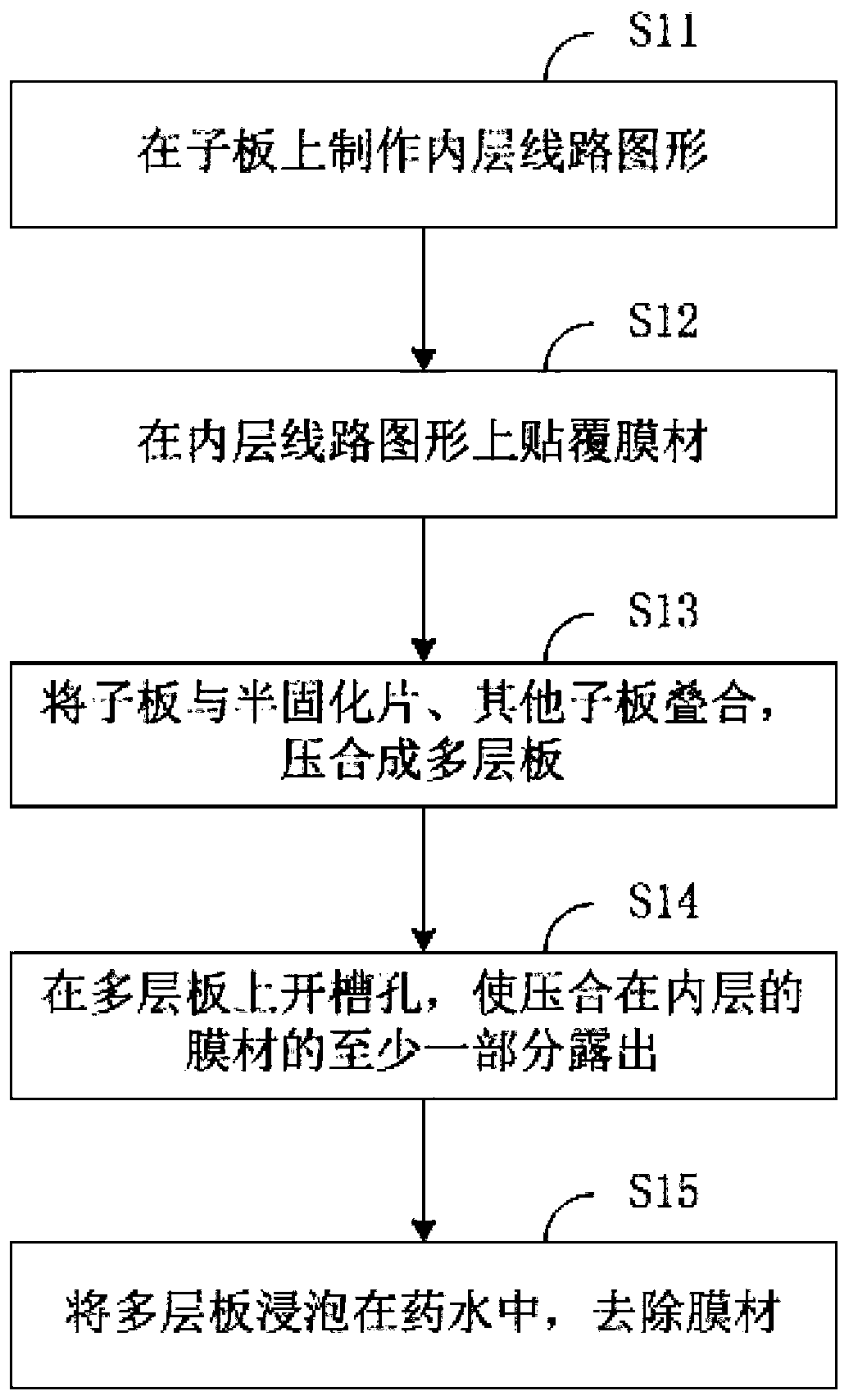
[0037] figure 1 It is a flow chart of the PCB manufacturing method provided by the embodiment of the present invention. Such as figure 1 As shown, the preparation method includes the following steps:

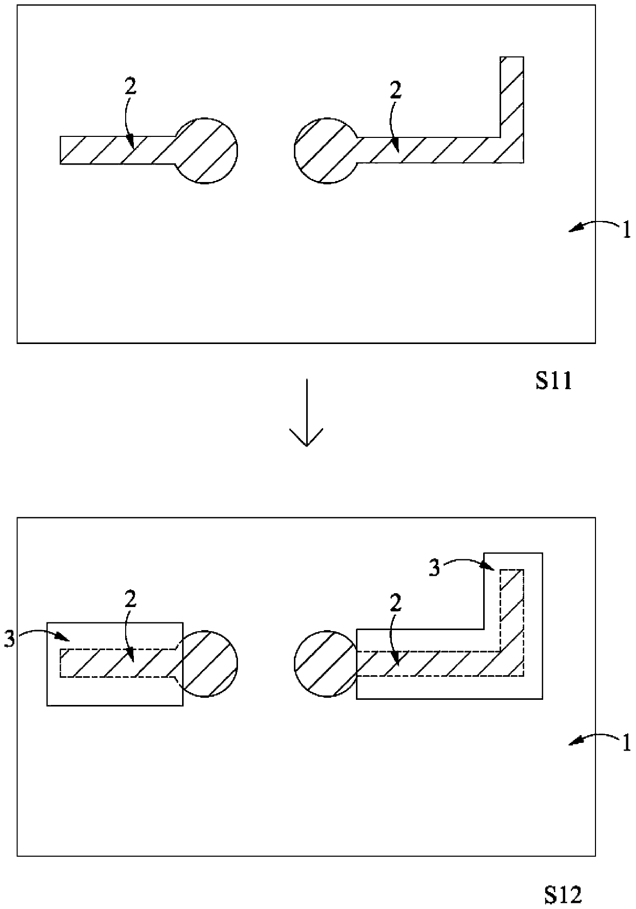
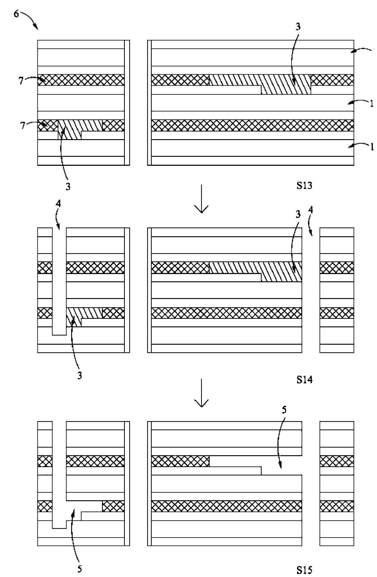
[0038] S11, making an inner layer circuit patte...


PUM


Abstract

The invention discloses a PCB manufacturing method, which relates to a manufacturing technology of a printed circuit board. The manufacturing method comprises the following steps of: manufacturing aninner layer circuit pattern on a daughter board, pasting a film material on the inner layer circuit pattern, superposing the daughter board with prepregs and other daughter boards, and pressing the daughter board, prepregs and other daughter boards into a multilayer board, forming a slotted hole in the multi-layer board to enable at least one part of the film material laminated on the inner layerto be exposed, and soaking the multilayer board in a liquid medicine, and removing the film material. According to the PCB manufacturing method disclosed in the invention, one surface of the inner layer circuit pattern of the PCB is coated with the dissoluble film material, and the film material is dissolved after lamination, so that the inner layer circuit is located in the built-in cavity to replace a high-loss resin dielectric layer, and the signal transmission loss is reduced; meanwhile, the cavities can be manufactured in different inner layers according to circuit distribution design, diversification of PCB products is facilitated, the PCB is suitable for more product requirements, the peripheries of the cavities are provided with enough supporting design, and the capacity of the cavities for resisting external pressure can be enhanced.

Description

technical field [0001] The invention relates to a manufacturing technology of a printed circuit board, in particular to a manufacturing method of a PCB. Background technique [0002] With the rapid development of 5G technology, the frequency of signal transmission is getting higher and higher. For PCB products, how to reduce the transmission loss of high-speed and high-frequency signals is a key research topic in the industry. In the prior art, methods such as selecting low-loss boards and using low-roughness potions to treat the surface of the circuit are used. However, when the upper and lower layers of the inner layer are covered by a dielectric layer, the signal loss of the PCB produced by the existing technology is still very large, which cannot meet the requirements of wireless radio frequency products above 70 GHz, which is not conducive to signal transmission and reception. Contents of the invention [0003] The purpose of the present invention is to propose a met...

Claims


Application Information

Patent Timeline
Patent Type & Authority Applications(China)
IPC IPC(8): H05K3/46H05K3/42H05K1/02
CPCH05K1/024H05K3/429H05K3/4602H05K3/4697H05K2203/0793
Inventor 王洪府肖璐孙改霞傅宝林
Owner DONGGUAN SHENGYI ELECTRONICS
Why Eureka
Try Eureka