Semiconductor memory structure and manufacturing method of bit line contact part thereof

A manufacturing method and contact technology, which are applied in the manufacture of semiconductor/solid-state devices, semiconductor devices, electric solid-state devices, etc., can solve the problems of increased bit line contact resistance, short circuit of bit lines, etc., and achieve the prevention of resistance increase, The effect of avoiding short circuit of the bit line and increasing the process window

Pending Publication Date: 2019-12-27
CHANGXIN MEMORY TECH INC
View PDF0 Cites 0 Cited by
  • Summary
  • Abstract
  • Description
  • Claims
  • Application Information

AI Technical Summary

Problems solved by technology

[0010] In view of the above-mentioned shortcomings of the prior art, the object of the present invention is to provide a semiconductor storage structure and a method for manufacturing the bit line contact portion thereof, which is used to solve the problem of the bit line contact caused by the contact material not being completely etched in the prior art. Short circuit, or the problem of increased contact resistance of the bit line due to over-etching of the contact material

Method used


Image

  • Semiconductor memory structure and manufacturing method of bit line contact part thereof
  • Semiconductor memory structure and manufacturing method of bit line contact part thereof
  • Semiconductor memory structure and manufacturing method of bit line contact part thereof

Examples


Embodiment 1

[0097] The present invention provides a method for manufacturing a bit line contact portion, comprising the following steps:

[0098] Such as Figure 10 As shown, step S1 is performed: providing a substrate 201 on which an etch stop layer 202 is formed.

[0099] Specifically, the substrate 201 may use conventional semiconductor materials such as Si, SiGe, SOI, etc. In this embodiment, the substrate 201 takes a silicon substrate as an example.

[0100] Specifically, an isolation structure 203 is further formed in the substrate 201 , and the isolation structure 203 defines a plurality of active regions 214 in the substrate 201 . In this embodiment, the isolation structure 203 is a shallow trench isolation structure (STI). According to the requirements of different semiconductor storage structures, the active region can adopt different layouts, and the protection scope of the present invention should not be excessively limited here.

[0101] Specifically, the etching stop laye...

Embodiment 2

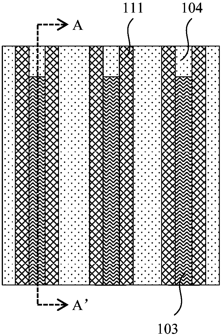
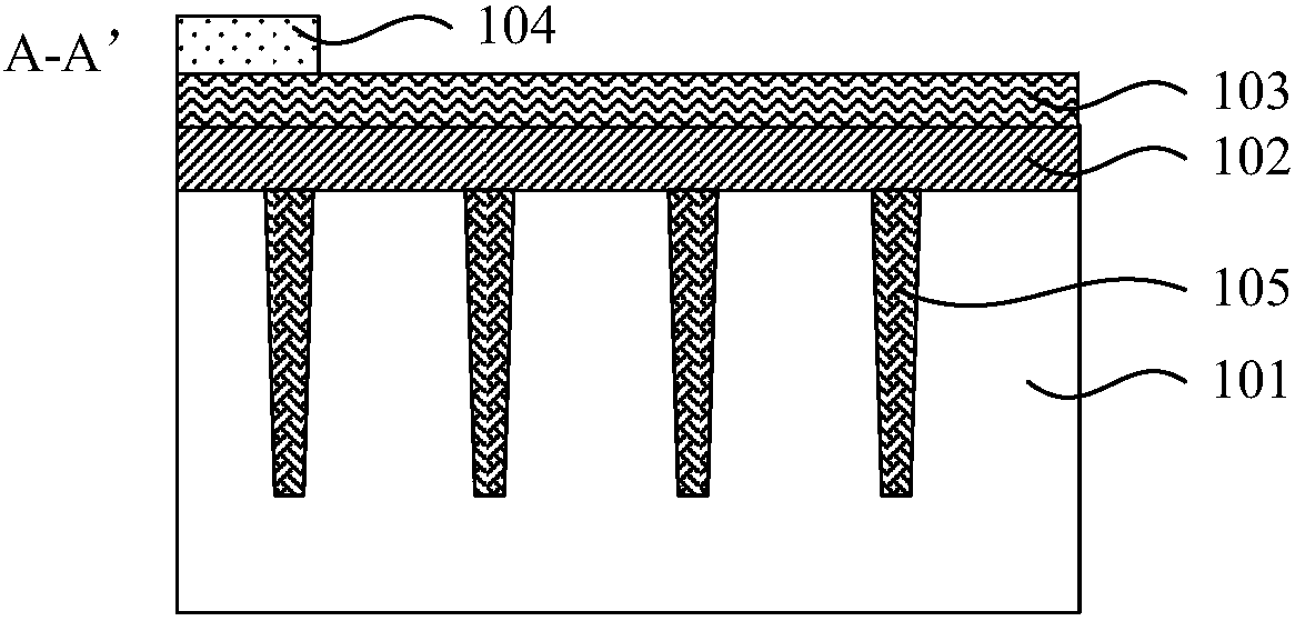
[0125] Such as Figure 20 and Figure 21 As shown, the present invention also provides a semiconductor memory structure, wherein, Figure 20 is shown as a top view of the semiconductor memory structure, Figure 21 shown as Figure 20 II' cross-sectional view of the shown structure, it can be seen that the semiconductor storage structure includes a substrate 201, a plurality of bit line contact isolation parts 205 of an etch stop layer, and a plurality of bit line contact parts 212 of a contact material and a plurality of bit lines 211 .

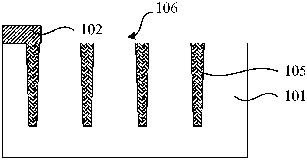
[0126] Specifically, a plurality of bit line contact isolation parts 205 are discretely arranged on the substrate 201 to isolate a plurality of bit line contact regions 215 in the substrate. In an extending direction, the substrate The upper surface of the bit line contact region and the top and side surfaces of the bit line contact isolation part form a contact material forming surface with a height difference.

[0127] Specifically, a ...


PUM

PropertyMeasurementUnit
Lengthaaaaaaaaaa
Thicknessaaaaaaaaaa

Abstract

The invention provides a semiconductor memory structure and a manufacturing method of a bit line contact part of the semiconductor memory structure. The manufacturing method is characterized in that abit line contact isolation part is firstly manufactured before a bit line contact material is deposited, so the bit line contact part is isolated by the bit line contact isolation part in the deposition stage, and the situation of bit line short circuit cannot be caused even if incomplete etching occurs in the subsequent etching process. The manufacturing method is advantaged in that the situation of bit line short circuit caused by incomplete etching of the contact material can be avoided, a process window of subsequent bit line etching is increased, and increase of resistance of bit line contact caused by over-etching of the contact material is further prevented.

Description

technical field [0001] The invention belongs to the field of semiconductor integrated circuits, and relates to a semiconductor memory structure and a manufacturing method of a bit line contact part thereof. Background technique [0002] In the semiconductor memory structure, there is a bit line contact portion under the bit line. The existing bit line contact manufacturing method includes the following steps: [0003] Step 1: If figure 1 and figure 2 As shown, a hard mask layer 103 is formed on the silicon nitride layer 102 on the surface of the substrate 101, a photoresist layer 104 is formed on the hard mask layer, and the photoresist layer is patterned, wherein the substrate is formed with a number of isolation structures 105, figure 1 presented as a top view showing the planar layout of wordlines 111, figure 2 shown as figure 1 The A-A' direction sectional view of the structure shown, and then as image 3 As shown, etching is used to transfer the pattern into th...

Claims


Application Information

Patent Timeline
IPC IPC(8): H01L27/108H01L21/8242
CPCH10B12/30H10B12/482H10B12/485
Inventor 不公告发明人
Owner CHANGXIN MEMORY TECH INC
Why Eureka
Try Eureka