Nano cold cathode electron source with dual gate-all-around structure and manufacturing method thereof
A cold cathode and electron source technology, applied in cold cathode manufacturing, electrode system manufacturing, discharge tube/lamp manufacturing, etc., can solve the problems of low field emission current of nano-cold cathodes, inability to manufacture large areas, and difficulty in manufacturing, etc. Achieve the effect of realizing large-area production, reducing electrode lead arrangement, and facilitating stable work
- Summary
- Abstract
- Description
- Claims
- Application Information
AI Technical Summary
Problems solved by technology
Method used
Image


Examples
Embodiment 1
[0047] In this example, a ZnO nanometer cold cathode electron source is prepared.
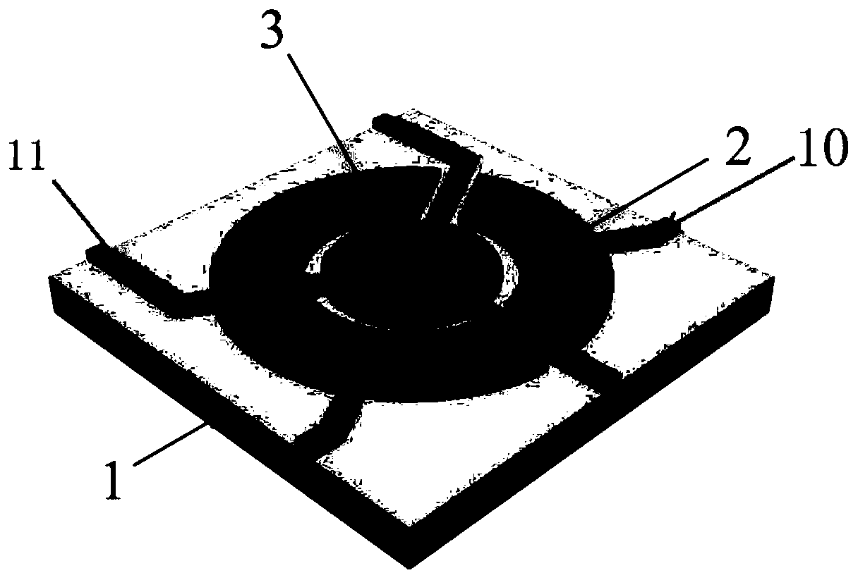
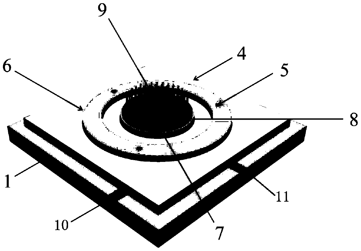
[0048] like Figure 1-Figure 3 As shown, the nano-cold cathode electron source of double-ring gate structure of the present invention comprises substrate 1, the bottom section annular gate electrode 2 and bottom cathode electrode 3 that are arranged on substrate 1, insulating layer 4, etched through hole 5. Top ring-shaped gate electrode 6, top cathode electrode 7, growth source film 8 and nanowire cold cathode 9.
[0049] The bottom segmented ring-shaped gate electrode 2 is a segmented and discontinuous ring-shaped electrode structure, which surrounds the bottom cathode electrode 3 , and the outer leads of the bottom segmented ring-shaped gate electrode 2 and the bottom cathode electrode 3 are arranged vertically. The insulating layer 4 covers the bottom section ring-shaped gate electrode 2 and the bottom cathode electrode 3, and the insulation layer 4 is etched with several etching through h...
Embodiment 2
[0059] In this embodiment, a CuO nanometer cold cathode electron source is prepared.
[0060] Clean and dry the substrate 1; the substrate 1 is a large-area glass substrate. On the substrate 1, make the bottom section ring-shaped grid electrode 2 and the bottom cathode electrode 3; the conductive film IZO as the bottom section ring-shaped grid electrode 2 and the bottom cathode electrode 3, the conductive film is passed through the magnetron Prepared by sputtering, UV lithography and etching processes. The thickness of the conductive film is 0.1 μm.
[0061] An insulating layer 4 is deposited on the bottom segmented annular gate electrode 2 and the bottom cathode electrode 3 . The insulating film used as the insulating layer 4 is silicon dioxide material, and the insulating layer 4 is prepared by chemical vapor deposition.
[0062] Localized etching of the insulating layer 4 on the insulating layer 4 results in etched vias 5 for connecting the top cathode electrode 7 with t...
Embodiment 3
[0067] In this embodiment, a TiO nanometer cold cathode electron source is prepared.
[0068] Clean and dry the substrate 1; the substrate 1 is a large-area glass substrate. On the substrate 1, make the bottom section ring-shaped grid electrode 2 and the bottom cathode electrode 3; the conductive film as the bottom section ring-shaped grid electrode 2 and the bottom cathode electrode 3 is AZO, and the conductive film is passed through magnetic Controlled sputtering, UV lithography and etching processes. The thickness of the conductive film is 2 μm.
[0069] An insulating layer 4 is deposited on the bottom segmented annular gate electrode 2 and the bottom cathode electrode 3 . The insulating film used as the insulating layer 4 is silicon dioxide material, and the insulating layer 4 is prepared by chemical vapor deposition.
[0070] Localized etching of the insulating layer 4 on the insulating layer 4 results in etched vias 5 for connecting the top cathode electrode 7 with th...
PUM
 Abstract
Description
Claims
Application Information
 - R&D
- Intellectual Property
- Life Sciences
- Materials
- Tech Scout
- Unparalleled Data Quality
- Higher Quality Content
- 60% Fewer Hallucinations
Browse by: Latest US Patents, China's latest patents, Technical Efficacy Thesaurus, Application Domain, Technology Topic, Popular Technical Reports.
© 2025 PatSnap. All rights reserved.Legal|Privacy policy|Modern Slavery Act Transparency Statement|Sitemap|About US| Contact US: help@patsnap.com