


Quick Research
Generate reliable direction feasibility study reports for your R&D in just a few steps.

Technical Q&A
Discover and master advanced knowledge NOW. Basics, ideas, possibilities, all at once.

Find Solutions
As an expert in R&D theories, this can generate solutions to your technical problems instantly.

Evaluate Feasibility
Analyze your overall solution with one click, know your potential R&D risks in advance.

Monitor Landscape
Get weekly tech updates, stay abreast of the latest tech innovations and key insights.
Method for preparing double-layer perovskite manganese oxide film material on monocrystalline silicon substrate through epitaxial growth
A double-layer perovskite and epitaxial growth technology, applied in the field of magnetic materials, can solve the problem of difficulty in synthesizing double-layer perovskite thin films, and achieve the effects of low cost and simple preparation
- Summary
- Abstract
- Description
- Claims
- Application Information
AI Technical Summary
Problems solved by technology
Method used
Image

Examples
Embodiment 1
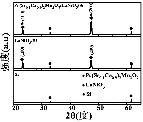
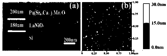
[0027] Using pulsed laser deposition technology, using Si(100) substrate as the substrate, LaNiO was sequentially deposited at 600 °C 3 thin film, deposited at 750°C on the top layer of Pr(Sr 0.1 Ca 0.9 ) 2 mn 2 o 7 film;
[0028] (1) Using the sol-gel method, calcining at 1200°C and 1400°C for 48 hours respectively, to prepare the LaNiO needed for the experiment 3 and Pr(Sr 0.1 Ca 0.9 ) 2 mn 2 o 7 target.
[0029] (2) Put the single crystal Si (100) substrate into the preparation chamber of the pulsed laser deposition system, and evacuate the preparation chamber of the pulsed laser deposition system to ≤5×10 -4 Pa, heating the substrate to 600°C, with LaNiO 3 The block material is used as the target material, the laser voltage is 23.0KV, the deposition rate is 3HZ, and the deposition times are 4000 times. In-situ annealing for 5 minutes, then continue to heat up to 750 ° C, with Pr (Sr 0.1 Ca 0.9 ) 2 mn 2 o 7 The block material is used as the target material...
Embodiment 2
[0032] Using pulsed laser deposition technology, using Si(100) substrate as the substrate, LaNiO was sequentially deposited at 650 °C 3 thin film, deposited at 750°C on the top layer of Pr(Sr 0.1 Ca 0.9 ) 2 mn 2 o 7 film;
[0033] (1) Using the sol-gel method, calcining at 1200°C and 1400°C for 48 hours respectively, to prepare the LaNiO needed for the experiment 3 and Pr(Sr 0.1 Ca 0.9 ) 2 mn 2 o 7 target.
[0034] (2) Put the single crystal Si(100) substrate into the preparation chamber of the pulsed laser deposition system, and vacuum the preparation chamber of the pulsed laser deposition system to ≤5×10 -4 Pa, heating the substrate to 650°C, with LaNiO 3 The block material is used as the target material, the laser voltage is 23.0KV, the deposition rate is 3HZ, and the deposition times are 4000 times. In-situ annealing for 5 minutes, then continue to heat up to 750 ° C, with Pr (Sr 0.1 Ca 0.9 ) 2 mn 2 o 7 The block material is used as the target material, t...
Embodiment 3
[0037] Using pulsed laser deposition technology, using Si(100) substrate as the substrate, LaNiO was sequentially deposited at 700 °C 3 thin film, deposited at 750°C on the top layer of Pr(Sr 0.1 Ca 0.9 ) 2 mn 2 o 7 film;
[0038] (1) Using the sol-gel method, calcining at 1200°C and 1400°C for 48 hours respectively, to prepare the LaNiO needed for the experiment 3 and Pr(Sr 0.1 Ca 0.9 ) 2 mn 2 o 7 target.
[0039] (2) Put the single crystal Si(100) substrate into the preparation chamber of the pulsed laser deposition system, and vacuum the preparation chamber of the pulsed laser deposition system to ≤5×10 -4 Pa, heating the substrate to 700°C, with LaNiO 3 The block material is used as the target material, the laser voltage is 23.0KV, the deposition rate is 3HZ, and the deposition times are 4000 times. In-situ annealing for 5 minutes, then continue to heat up to 750 ° C, with Pr (Sr 0.1 Ca 0.9 ) 2 mn 2 o 7 The block material is used as the target material, t...
PUM
| Property | Measurement | Unit |
|---|---|---|
| thickness | aaaaa | aaaaa |
| thickness | aaaaa | aaaaa |
| thickness | aaaaa | aaaaa |
Abstract
Description
Claims
Application Information
 - R&D Engineer
- R&D Manager
- IP Professional
- Industry Leading Data Capabilities
- Powerful AI technology
- Patent DNA Extraction
Browse by: Latest US Patents, China's latest patents, Technical Efficacy Thesaurus, Application Domain, Technology Topic, Popular Technical Reports.
© 2024 PatSnap. All rights reserved.Legal|Privacy policy|Modern Slavery Act Transparency Statement|Sitemap|About US| Contact US: help@patsnap.com