A kind of SRAM and its manufacturing method and electronic device
A manufacturing method and technology of fins, which are applied in semiconductor/solid-state device manufacturing, circuits, electrical components, etc., can solve the problems of asymmetrical layout of SRAM and severe local changes of transmission gate transistors, etc., so as to improve performance and yield, and local fluctuations Reduced, process-control-friendly effects
- Summary
- Abstract
- Description
- Claims
- Application Information
AI Technical Summary
Problems solved by technology
Method used
Image
Examples
Embodiment 1
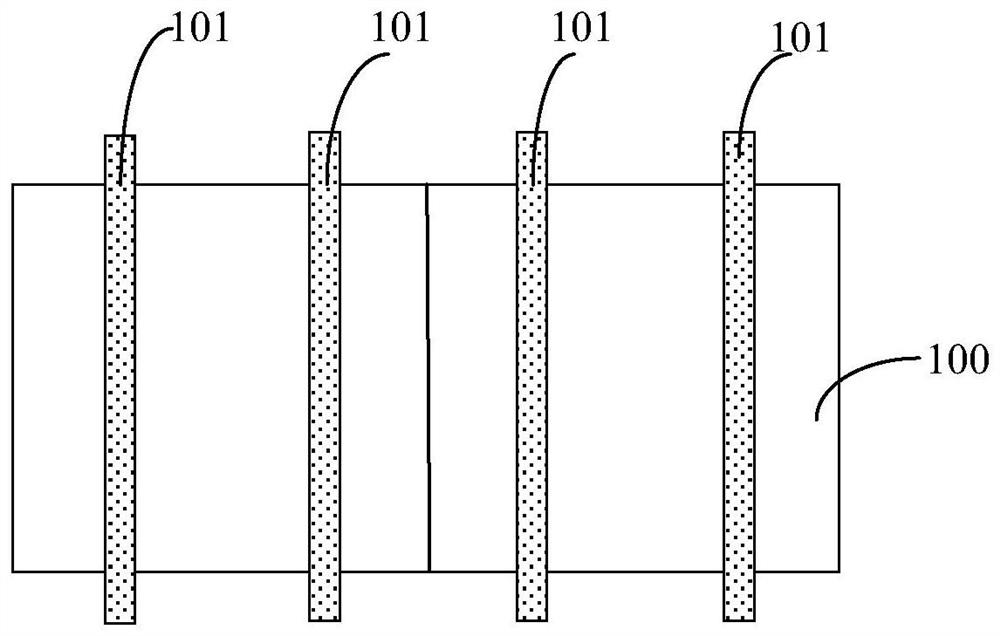
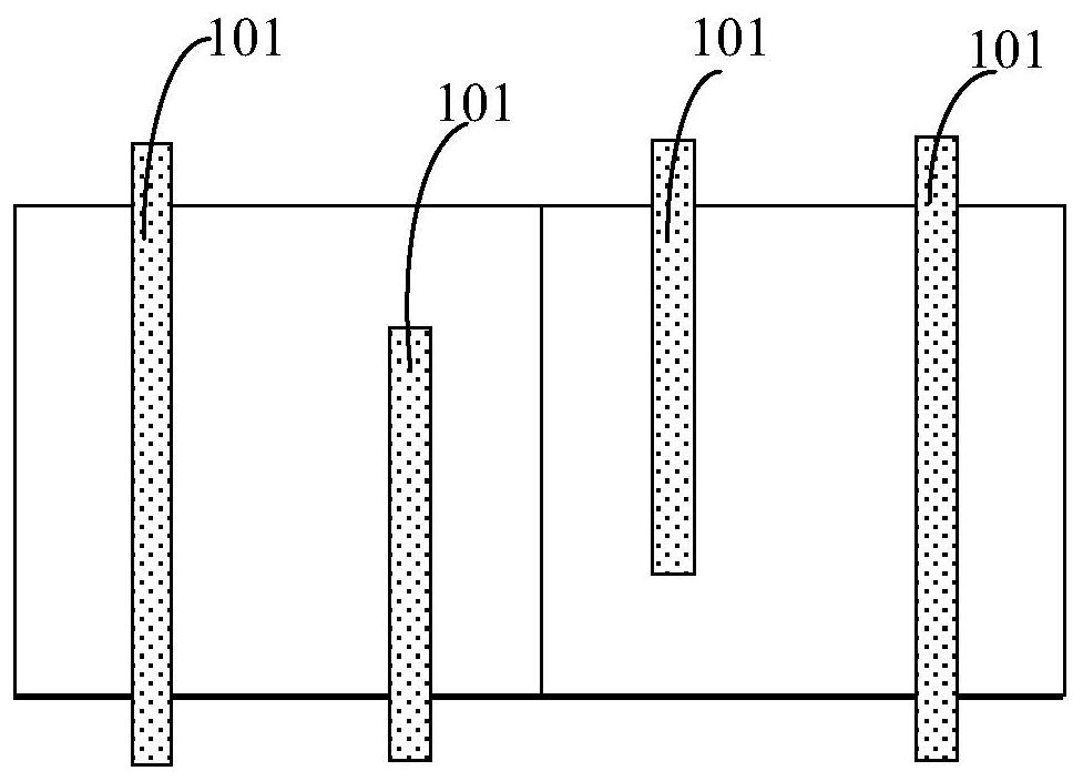
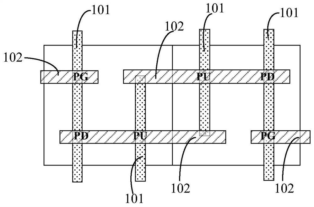
[0080] Below, refer to figure 2 , Figure 3A to Figure 3D as well as Figure 4A to Figure 4C The manufacturing method of the SRAM of the present invention is described in detail.
[0081] As an example, the manufacturing method of the SRAM of the present invention includes:
[0082] First, perform step 1, such as Figure 3A As shown, a semiconductor substrate 200 is provided, on which a first fin structure 2011, a second fin structure 2012, a third fin structure 2013 and a fourth fin structure 2014 are formed, wherein adjacent The projection of the fin structure on the surface of the semiconductor substrate 200 is symmetrical about the center line between the two, for example, as Figure 3A As shown, the projections of the first fin structure 2011 and the second fin structure 2012 on the surface of the semiconductor substrate 200 are symmetrical about the center line 11 between them, and the third fin structure 2013 and the fourth fin structure 2014 are in The projection...
Embodiment 2
[0163] The present invention also provides a SRAM prepared by the method of the first embodiment above. Below, refer to Figure 3D with Figure 4C The structure of the SRAM of the present invention will be described in detail, and since the SRAM device in this embodiment is prepared by the aforementioned method, some same structures will not be described repeatedly.
[0164] As an example, such as Figure 3D with Figure 4C As shown, the SRAM of the present invention includes a semiconductor substrate 200 .
[0165] Exemplarily, a first fin structure 2011, a second fin structure 2012, a third fin structure 2013 and a fourth fin structure 2014 are formed on the semiconductor substrate 200, wherein the adjacent fin structures The projection on the surface of the semiconductor substrate 200 is symmetrical about the center line between the two, for example, as Figure 3A As shown, the projections of the first fin structure 2011 and the second fin structure 2012 on the surface...
Embodiment 3
[0195] Another embodiment of the present invention also provides an electronic device, including the aforementioned SRAM, which is prepared according to the aforementioned method.
[0196] The electronic device of this embodiment can be any electronic device such as a mobile phone, a tablet computer, a notebook computer, a netbook, a game console, a TV set, a VCD, a DVD, a navigator, a digital photo frame, a camera, a video camera, a recording pen, MP3, MP4, PSP, etc. Product or equipment, but also any intermediate product including electrical circuits. The electronic device of the embodiment of the present invention has better performance due to the use of the above-mentioned SRAM.
[0197] in, Image 6 An example of a mobile phone handset is shown. The mobile phone handset 300 is provided with a display portion 302 included in a casing 301, operation buttons 303, an external connection port 304, a speaker 305, a microphone 306, and the like.
[0198]Wherein, the mobile ph...
PUM
| Property | Measurement | Unit |
|---|---|---|
| thickness | aaaaa | aaaaa |
| thickness | aaaaa | aaaaa |
Abstract
Description
Claims
Application Information
 - R&D Engineer
- R&D Manager
- IP Professional
- Industry Leading Data Capabilities
- Powerful AI technology
- Patent DNA Extraction
Browse by: Latest US Patents, China's latest patents, Technical Efficacy Thesaurus, Application Domain, Technology Topic, Popular Technical Reports.
© 2024 PatSnap. All rights reserved.Legal|Privacy policy|Modern Slavery Act Transparency Statement|Sitemap|About US| Contact US: help@patsnap.com


