Near-infrared light regulation synaptic transistor and preparation method thereof
A near-infrared light and transistor technology, which is applied in semiconductor/solid-state device manufacturing, semiconductor devices, electrical components, etc., can solve problems such as limited choices and achieve the effect of rich choices
- Summary
- Abstract
- Description
- Claims
- Application Information
AI Technical Summary
Problems solved by technology
Method used
Image
Examples
preparation example Construction
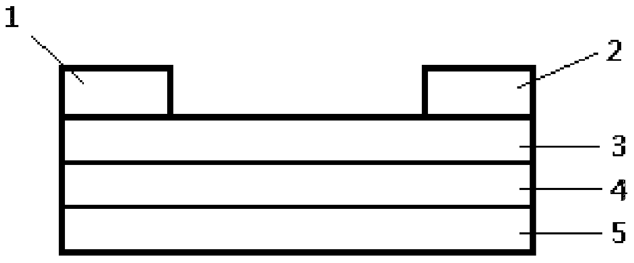
[0035] The present invention also provides a method for preparing a near-infrared light-regulated synaptic transistor, comprising the following steps:
[0036] Step S1, setting MoSe on the substrate layer 2 / Bi 2 Se 3 / PMMA layer, where the MoSe 2 / Bi 2 Se 3 / PMMA layer is MoSe 2 / Bi 2 Se 3 A mixture of heterostructure and PMMA in chlorobenzene solution was prepared.
[0037] Step S2, in MoSe 2 / Bi 2 Se 3 A semiconductor layer is provided on the / PMMA layer.
[0038] Step S3, disposing a source and a drain on the semiconductor layer.
[0039] The concentration of the chlorobenzene solution of PMMA in the step S1 is 8-12 mg / ml, preferably 10 mg / ml.
[0040] MoSe in the step S1 2 / Bi 2 Se 3 The preparation method of the heterostructure is a thermal injection method, which specifically includes the following steps:
[0041] Step S11, Ph 3 Bi and (PhCH 2 ) 2 Se 2 Dissolved in oleylamine, sonicated to obtain the first mixed solution, the Ph 3 Bi, (PhCH 2 ) 2...
Embodiment 1
[0055] 0.05mol of Ph 3 Bi with 0.0375mol of (PhCH 2 ) 2 Se 2 Dissolve in 0.5mL, that is, 0.0015mol oleylamine, and perform ultrasonic treatment to obtain the first mixed solution. 0.05mol of MoO 2 (acac) 2 With 0.05mol of (PhCH 2 ) 2 Se 2Dissolve in 0.5 mL, namely 0.0015 mol oleylamine, and perform ultrasonic treatment to obtain the second mixed solution. Put the first mixed solution and the second mixed solution into an oven at 70 degrees centigrade and heat for 4 minutes. 5 ml of oleylamine and 0.5 ml of oleic acid were placed in a 100 ml three-necked round-bottomed flask, heated, kept at 140 degrees Celsius for 30 minutes, and then removed under the conditions of strong magnetic stirring and pure argon flow. The first mixed solution is quickly added to the reactor by a syringe equipped with a needle, reacted for 5 minutes at 280 degrees Celsius, and then the second mixed solution is quickly added to the reactor by a syringe equipped with a needle, reacted for 20 mi...
Embodiment 2
[0058] 0.04mol of Ph 3 Bi with 0.040mol of (PhCH 2 ) 2 Se 2 Dissolve in 0.5mL, that is, 0.0015mol oleylamine, and perform ultrasonic treatment to obtain the first mixed solution. 0.06mol of MoO 2 (acac) 2 With 0.04mol of (PhCH 2 ) 2 Se 2 Dissolve in 0.5 mL, namely 0.0015 mol oleylamine, and perform ultrasonic treatment to obtain the second mixed solution. Put the first mixed solution and the second mixed solution into an oven at 60 degrees centigrade and heat for 5 minutes. 3.6 milliliters of oleylamine and 0.4 milliliters of oleic acid were placed in a 100 milliliter three-necked round-bottomed flask, heated, kept at 130 degrees Celsius for 30 minutes, and then removed under conditions of strong magnetic stirring and pure argon flow. The first mixed solution is quickly added to the reactor by a syringe equipped with a needle, reacted for 6 minutes at 270 degrees Celsius, and then the second mixed solution is quickly added to the reactor by a syringe equipped with a n...
PUM
 Abstract
Description
Claims
Application Information
 - R&D
- Intellectual Property
- Life Sciences
- Materials
- Tech Scout
- Unparalleled Data Quality
- Higher Quality Content
- 60% Fewer Hallucinations
Browse by: Latest US Patents, China's latest patents, Technical Efficacy Thesaurus, Application Domain, Technology Topic, Popular Technical Reports.
© 2025 PatSnap. All rights reserved.Legal|Privacy policy|Modern Slavery Act Transparency Statement|Sitemap|About US| Contact US: help@patsnap.com


