
Patsnap Eureka
For R&D, Patsnap Eureka makes reading and utilizing patents & technical documents easy.
Patsnap Eureka AIR
Designed for self-driven R&D workflows. Generate viable solutions, solve complex R&D challenges, empower your innovation with AI.

Patsnap Eureka Materials
Designed for material experts only. Revolutionize your material R&D, from search, analyze, to developing new materials.

TechResearch
Generate reliable direction feasibility study reports for your R&D in just a few steps.

TechSeek
Discover and master advanced knowledge NOW. Basics, ideas, possibilities, all at once.

TechMind
As an expert in R&D Theories, TechMind can generates customized viable solutions instantly.

TechRisk
Analyze your overall solution with one click, know your potential R&D risks in advance.

TechMonitor
Get weekly tech updates, stay abreast of the latest tech innovations and key insights.
Etching method of sic substrate
A substrate and by-product technology, applied in the field of SiC substrate etching, can solve the problems of increasing the difficulty and workload of production and maintenance, and affecting the yield of products, so as to prolong the cleaning and maintenance cycle, reduce the difficulty and workload of maintenance, Possible effect of reducing deposition
- Summary
- Abstract
- Description
- Claims
- Application Information
AI Technical Summary
Problems solved by technology
Method used
Image

Examples
Embodiment
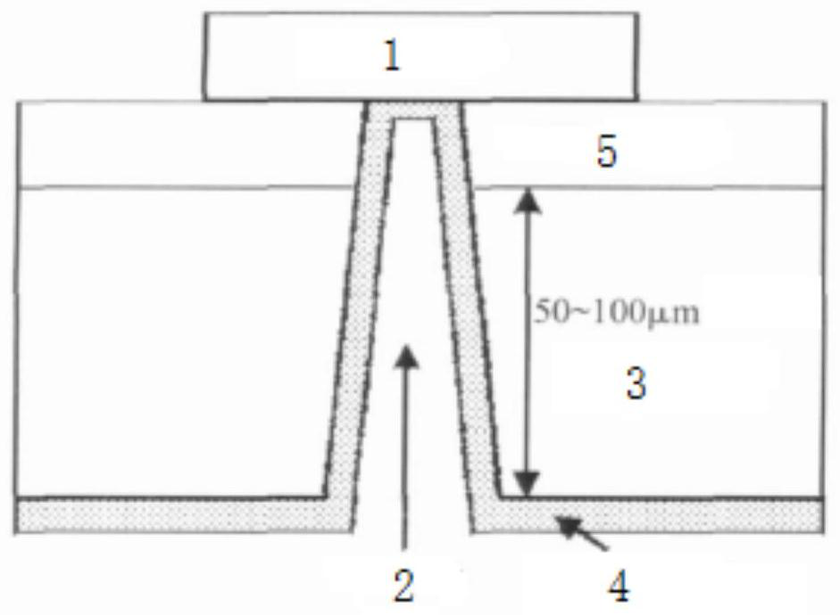
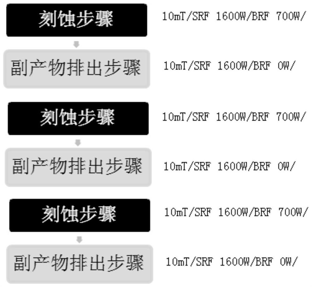
[0039] figure 2 A flowchart showing a method of etching a SiC substrate according to an exemplary embodiment of the present invention. The etching method of the SiC substrate alternately performs the etching step and the by-product discharge step, in the etching step, the SiC substrate provided in the reaction chamber is etched; in the by-product discharge step, the reaction in the reaction chamber is discharged The processes of the by-product, etching step and by-product discharge step are as follows:
[0040] Etching steps: 10mT / SRF 1600W / BRF 700W / 100SF 6 +30O 2 +20Ar / 10s, that is, the pressure of the reaction chamber is 10mT, the RF power of the upper electrode is 1600W, the RF power of the lower electrode is 700W, and the flow rate of the process gas is sulfur hexafluoride (SF 6 ) 100sccm, oxygen (O 2 ) 30sccm, argon (Ar) 20sccm, the duration is 10s;
[0041] By-product discharge steps: 10mT / SRF 1600W / BRF 0W / 150Ar / 1s, that is, the pressure of the reaction chamber is ...
PUM
 Abstract
Description
Claims
Application Information
 - R&D Engineer
- R&D Manager
- IP Professional
- Industry Leading Data Capabilities
- Powerful AI technology
- Patent DNA Extraction
Browse by: Latest US Patents, China's latest patents, Technical Efficacy Thesaurus, Application Domain, Technology Topic, Popular Technical Reports.
© 2024 PatSnap. All rights reserved.Legal|Privacy policy|Modern Slavery Act Transparency Statement|Sitemap|About US| Contact US: help@patsnap.com