Method for depositing aluminum nitride film on silicon substrate and silicon wafer

A technology of aluminum nitride film and silicon substrate, which is applied in the direction of semiconductor devices, electrical components, circuits, etc., can solve problems such as single method and cannot meet production needs, and achieve the effects of reducing costs, shortening production cycles, and enriching the market

Active Publication Date: 2019-12-03
BEIJING NAURA MICROELECTRONICS EQUIP CO LTD
View PDF3 Cites 5 Cited by
  • Summary
  • Abstract
  • Description
  • Claims
  • Application Information

AI Technical Summary

Problems solved by technology

[0004] At present, the method of depositing aluminum nitride thin films on silicon substrates is relatively simple, which cannot meet the production needs

Method used


Image

  • Method for depositing aluminum nitride film on silicon substrate and silicon wafer

Examples


Embodiment Construction

[0025] Specific embodiments of the present invention will be described in detail below in conjunction with the accompanying drawings. It should be understood that the specific embodiments described here are only used to illustrate and explain the present invention, and are not intended to limit the present invention.

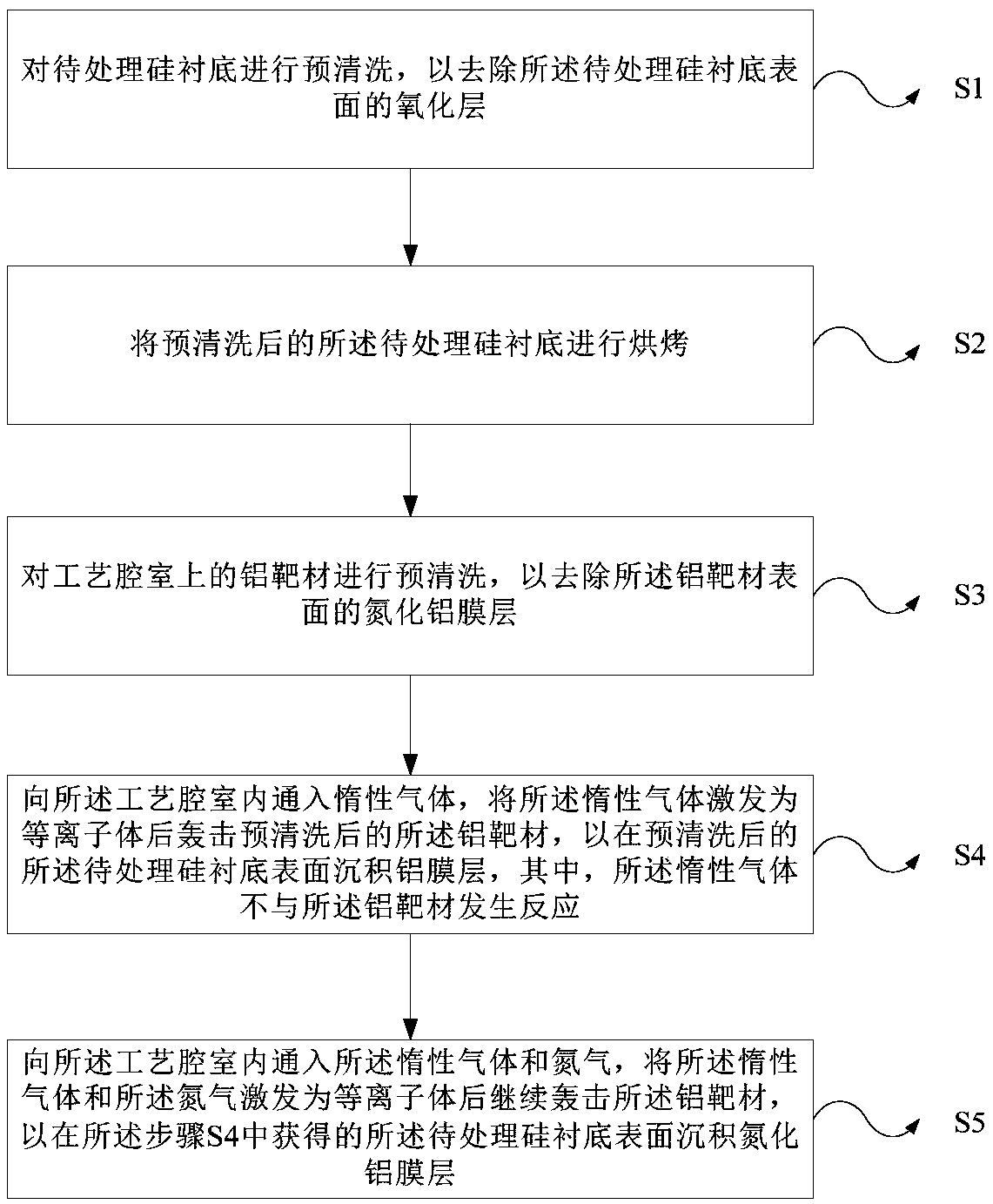
[0026] As one aspect of the present invention, a method for depositing an aluminum nitride film on a silicon substrate is provided, wherein, as figure 1 shown, including the following steps:

[0027] Step S1, pre-cleaning the silicon substrate to be processed, so as to remove the oxide layer on the surface of the silicon substrate to be processed;

[0028] Step S2, baking the pre-cleaned silicon substrate to be processed;

[0029] Step S3, pre-cleaning the aluminum target on the process chamber to remove the aluminum nitride film on the surface of the aluminum target;

[0030] Step S4, injecting an inert gas into the process chamber, exciting the inert gas in...


PUM


Abstract

The invention provides a method for depositing an aluminum nitride film on a silicon substrate. The method comprises the steps of: S1, carrying out the pre-cleaning of a to-be-processed silicon substrate so as to remove an oxidation layer on the surface of the to-be-processed silicon substrate; S2, baking the pre-cleaned to-be-processed silicon substrate; S3, pre-cleaning an aluminum target material on a process chamber to remove an aluminum nitride film layer on the surface of the aluminum target material; S4, introducing inert gas into the process chamber, exciting the inert gas into plasma,and bombarding the pre-cleaned aluminum target material to deposit an aluminum film layer on the surface of the pre-cleaned to-be-processed silicon substrate, the inert gas not reacting with the aluminum target material; and S5, introducing inert gas and nitrogen into the process chamber, exciting the inert gas and the nitrogen into plasma, and continuously bombarding the aluminum target materialto deposit an aluminum nitride film layer on the surface of the to-be-processed silicon substrate obtained in the step S4. The invention also provides a silicon wafer. The method can be used for preparing the aluminum nitride film layer with high crystallization quality on the silicon substrate.

Description

technical field [0001] The invention relates to the field of semiconductor technology, in particular to a method for depositing an aluminum nitride film on a silicon substrate and a silicon chip. Background technique [0002] In the prior art, a metal compound film layer is prepared on a substrate by a Metal Organic Chemical Vapor Deposition (MOCVD: Metal Organic Chemical Vapor Deposition) method. [0003] For example, when using metal-organic chemical vapor deposition method to prepare aluminum nitride film layer on silicon substrate, the usual process is to feed ammonia gas and trimethylaluminum, and at high temperature, through the chemical reaction of the two, silicon An aluminum nitride film layer is formed on the substrate. [0004] At present, the method of depositing aluminum nitride thin films on silicon substrates is relatively simple, which cannot meet the production requirements. Therefore, how to design a new method for depositing an aluminum nitride film on a...

Claims


Application Information

Patent Timeline
Patent Type & Authority Applications(China)
IPC IPC(8): H01L21/02H01L29/06
CPCH01L21/02043H01L21/0254H01L21/0262H01L21/02658
Inventor 王军董博宇李丽郭冰亮马怀超武学伟王桐徐宝岗刘绍辉张鹤南孙颖
Owner BEIJING NAURA MICROELECTRONICS EQUIP CO LTD
Why Eureka
Try Eureka