A high-speed and low-loss multi-slot gate high-voltage power device
A high-voltage power device, low-loss technology, applied in semiconductor devices, electrical components, circuits, etc., can solve the problems that devices are not easy to use in parallel, increase process difficulty and cost, and reduce reliability, and achieve enhanced injection efficiency and anti-latch. capability, the effect of eliminating the snapback phenomenon, and low turn-off loss
- Summary
- Abstract
- Description
- Claims
- Application Information
AI Technical Summary
Problems solved by technology
Method used
Image
Examples
Embodiment 1
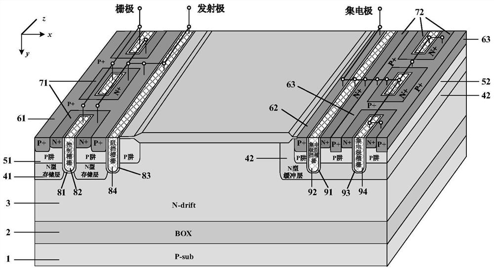
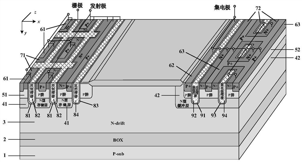
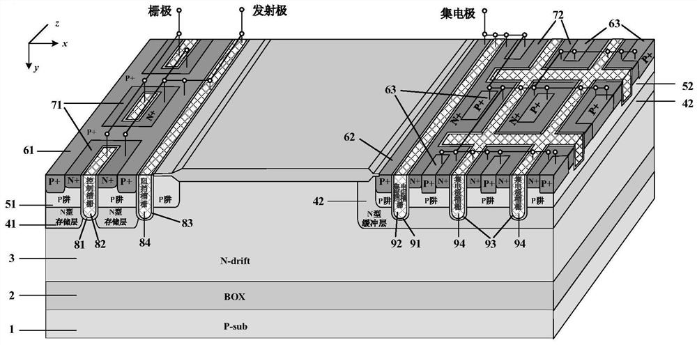
[0016] Such as figure 1 As shown, the multi-groove gate SOI LIGBT of this example includes a bottom-up substrate layer 1, an insulating dielectric layer 2, and an N-type drift region 3; one end of the N-type drift region 3 includes an emitter structure and an emitter groove structure, and the other end includes a collector structure and a collector tank structure.
[0017] The emitter structure includes a P well region 51, a P+ body contact region 61, and an N+ emitter region 71; the P+ body contact region 61 and the N+ emitter region 71 are located on the top of the P well region 51, and the P+ body The common lead end of the contact region 61 and the N+ emitter region 71 is the emitter; the collector structure includes the N-type buffer layer 42, the P well region 52, the P+ collector region 62, the N+ collector region 72 and the P well region 52 The body contacts the P+ region 63, the N-type buffer layer 42 is located on the top of the N-type drift region 3, the P well reg...
Embodiment 2
[0024] Such as Figure 6 Shown, in this example and embodiment 1 figure 1 The difference is that in this example, a P-type buried layer 53 is introduced under the trench gate structure at the emitter terminal. The working mechanism of device shutdown in this embodiment is consistent with that of Embodiment 1, the difference is that: when conducting forward conduction, the P-type buried layer 53 introduced in this example can assist in depleting the N-type storage layer 41, thereby improving the efficiency of the N-type storage layer. 41 Optimize the doping concentration and enhance the carrier storage effect, so in this example, the carrier concentration in the drift region of the device is higher, and the conduction voltage drop can be further reduced; at the same time, in the blocking state, the P-type buried layer 53 can also The electric field peak at the bottom of the emitter terminal groove structure is reduced, and the reliability of the device is improved. Therefore,...
PUM
 Abstract
Description
Claims
Application Information
 - R&D
- Intellectual Property
- Life Sciences
- Materials
- Tech Scout
- Unparalleled Data Quality
- Higher Quality Content
- 60% Fewer Hallucinations
Browse by: Latest US Patents, China's latest patents, Technical Efficacy Thesaurus, Application Domain, Technology Topic, Popular Technical Reports.
© 2025 PatSnap. All rights reserved.Legal|Privacy policy|Modern Slavery Act Transparency Statement|Sitemap|About US| Contact US: help@patsnap.com


