Display panel, display device and manufacturing method thereof
A display panel and display area technology, applied in the direction of electrical components, diodes, electric solid devices, etc., can solve the problems of poor display effect and low light penetration ability, so as to improve the transparent display effect, enhance the penetration ability, and ensure The effect of electrical properties
- Summary
- Abstract
- Description
- Claims
- Application Information
AI Technical Summary
Problems solved by technology
Method used
Image

Examples
Embodiment 1
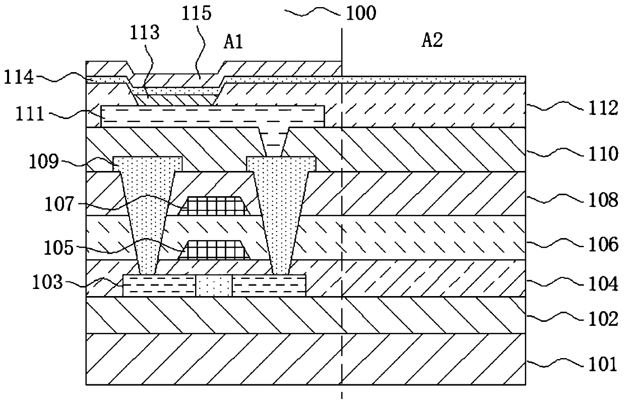
[0037] The disclosed embodiment provides a display panel 100, which is combined with figure 1 Describe in detail.
[0038] Such as figure 1 as shown, figure 1 A schematic cross-sectional structure diagram of a display panel 100 provided in an embodiment of the present disclosure, the display panel 100 includes a display area, figure 1 All shown in the above are display areas, and the display area includes a light-emitting sub-area A1 and an external light-transmitting sub-area A2, the light-emitting sub-area A1 is used for the normal display of the display panel, and the external light-transmitting sub-area A2 It is used to provide a path for external light to pass through when the display panel 100 is not performing a normal display function, so as to realize the display effect of the transparent display of the display panel 100 .
[0039] In this embodiment, the display panel 100 includes a base substrate 101, a buffer layer 102 disposed on the substrate 101; a polysilico...
Embodiment 2
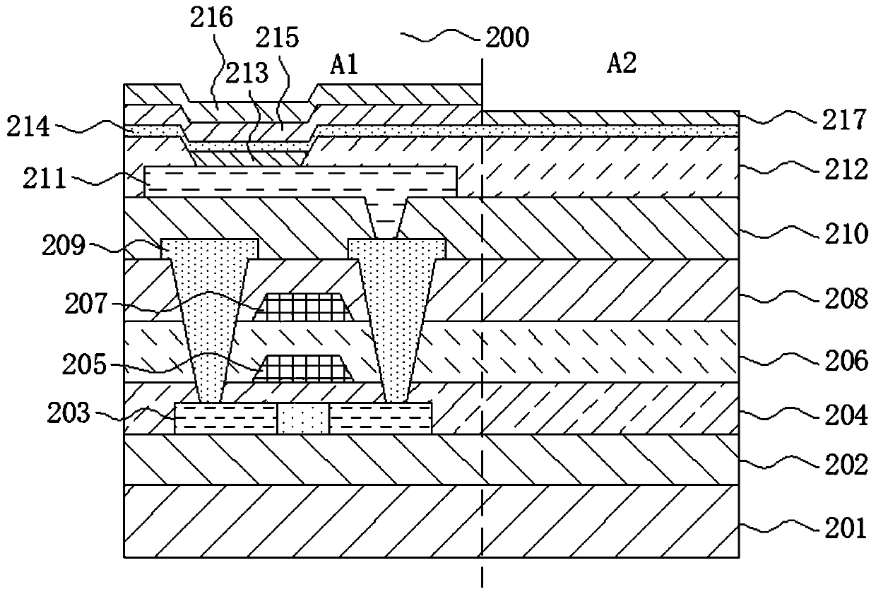
[0047] The disclosed embodiment provides a display panel, which is combined with figure 2 Describe in detail.
[0048] Such as figure 2 as shown, figure 2 A schematic cross-sectional structure diagram of a display panel 200 provided in an embodiment of the present disclosure, the display panel 200 includes a display area, figure 2 All shown in the figure are display areas, and the display area includes a light-emitting sub-area A1 and an external light-transmitting sub-area A2, the light-emitting sub-area A1 is used for the display panel 200 to normally display luminescence, and the external light transmitting sub-area A2 is used to provide a path for external light to pass through when the display panel 200 is not performing a normal display function, so as to realize the transparent display effect of the display panel 200 .
[0049] In this embodiment, the display panel 200 includes a base substrate 201, a buffer layer 202 disposed on the substrate 201; a polysilicon ...
Embodiment 3
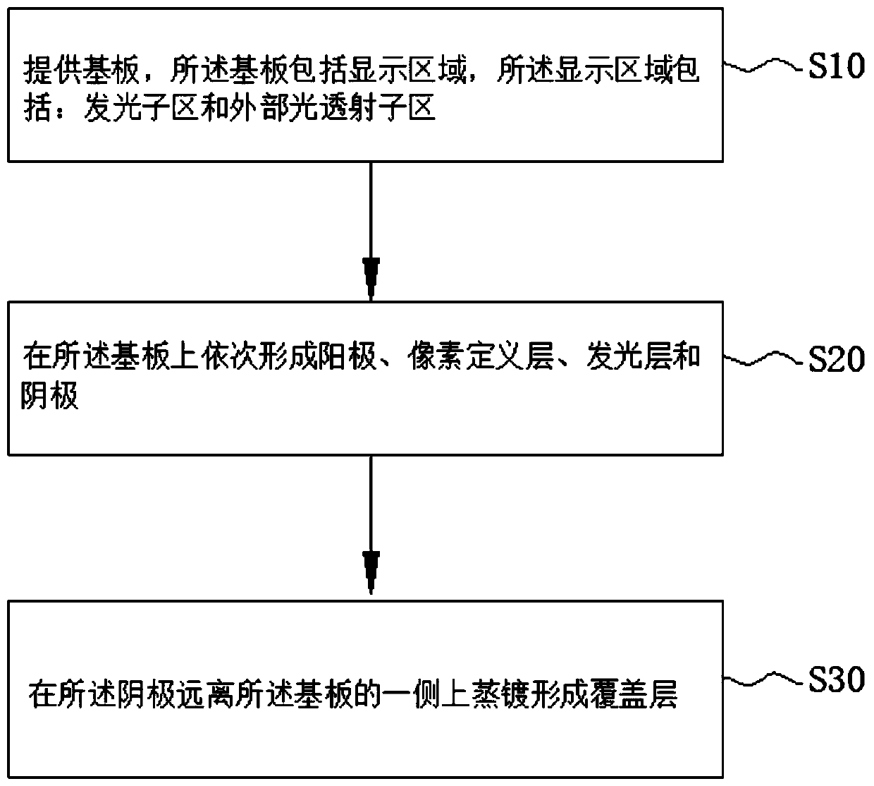
[0057] The embodiment of the present disclosure provides a method for manufacturing the display device 300, which is combined with image 3 , Figure 4A to Figure 4C Describe in detail.
[0058] Such as image 3 as shown, image 3 A schematic flow chart of the manufacturing method of the display device 300 provided by the disclosed embodiment, Figure 4A to Figure 4C A schematic cross-sectional structure diagram of a display device 300 provided in an embodiment of the present disclosure, the method includes:
[0059] Step S10 : providing a substrate 301 , the substrate 301 includes a display area, and the display area includes: a light-emitting sub-area A1 and an external light-transmitting sub-area A2 . Such as Figure 4A as shown, Figure 4A All shown in are display areas, the left side of the dotted line is the light-emitting sub-area A1, and the right side of the dotted line is the external light transmission sub-area A2, the light-emitting sub-area A1 is used for no...
PUM
 Abstract
Description
Claims
Application Information
 - R&D
- Intellectual Property
- Life Sciences
- Materials
- Tech Scout
- Unparalleled Data Quality
- Higher Quality Content
- 60% Fewer Hallucinations
Browse by: Latest US Patents, China's latest patents, Technical Efficacy Thesaurus, Application Domain, Technology Topic, Popular Technical Reports.
© 2025 PatSnap. All rights reserved.Legal|Privacy policy|Modern Slavery Act Transparency Statement|Sitemap|About US| Contact US: help@patsnap.com