Transparent oled display and manufacturing method thereof

A manufacturing method and display technology, applied in semiconductor/solid-state device manufacturing, semiconductor devices, electric solid-state devices, etc., can solve the problem of affecting the electrical performance and service life of terminal 930, reducing the transparent display effect of transparent OLED displays, and wasting light-transmitting area To achieve good transparent display effect, improve transparent display effect, improve electrical performance and service life

Active Publication Date: 2019-10-01
SHENZHEN CHINA STAR OPTOELECTRONICS SEMICON DISPLAY TECH CO LTD
View PDF5 Cites 0 Cited by
  • Summary
  • Abstract
  • Description
  • Claims
  • Application Information

AI Technical Summary

Problems solved by technology

[0006] The gate 210, active layer 400, source 610, drain 620, anode 910, OLED light-emitting layer 950, and cathode 960 are located in the TFT region, and the first storage capacitor electrode 220 and the second storage capacitor electrode 630 at C st In the region, since the first storage capacitor electrode 220 and the second storage capacitor electrode 630 are made of metal materials, C st area is opaque to light due to C st The area is relatively large, which wastes a certain light transmission area and aperture ratio, thereby reducing the transparent display effect of transparent OLED displays.
In addition, in the production process of the transparent OLED display, the connection terminal (Pad) 930 located in the peripheral area is usually prepared with the same material in the same process as the anode 910, and the connection terminal 930 and the anode 910 are both made of two layers of indium oxide A composite layer composed of a silver film 932 is interposed between the tin (ITO) films 931. Since the terminal 930 is located in the peripheral area of ​​the transparent OLED display and is exposed to the external environment, it is easy to contact water and oxygen, resulting in the connection terminal 930. The silver film 932 is corroded, thereby affecting the electrical performance and service life of the terminal 930

Method used


Image

  • Transparent oled display and manufacturing method thereof
  • Transparent oled display and manufacturing method thereof
  • Transparent oled display and manufacturing method thereof

Examples


Embodiment Construction

[0049] In order to further illustrate the technical means adopted by the present invention and its effects, the following describes in detail in conjunction with preferred embodiments of the present invention and accompanying drawings.

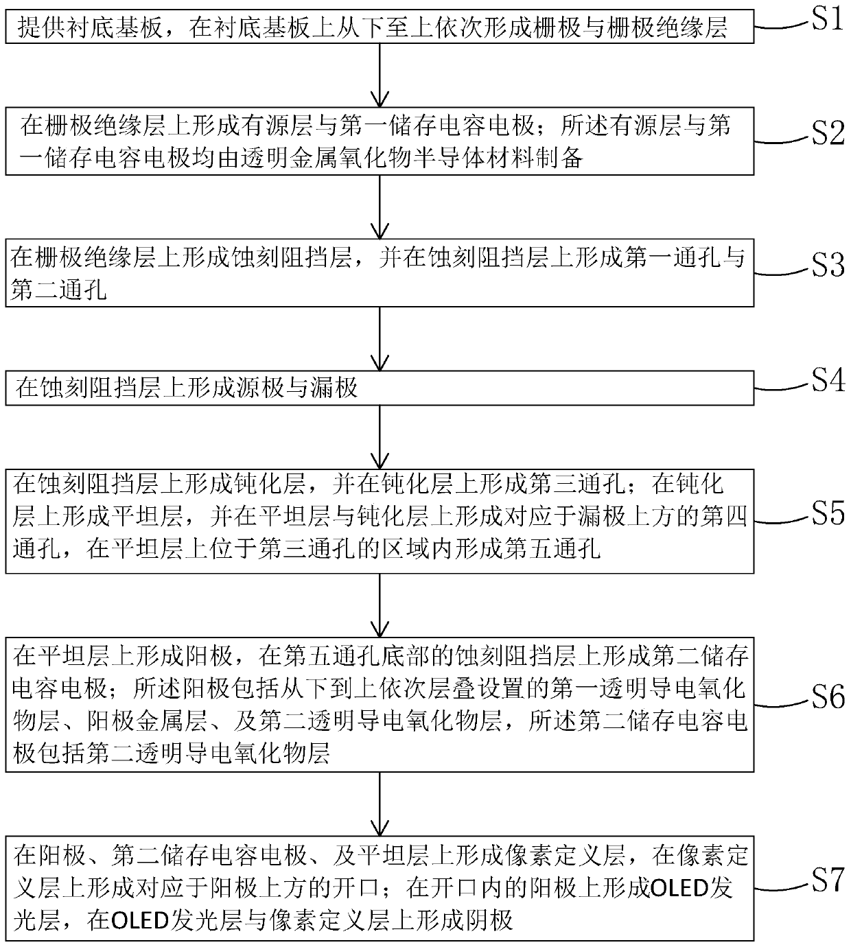
[0050] see image 3 , the invention provides a method for manufacturing a transparent OLED display, comprising the steps of:

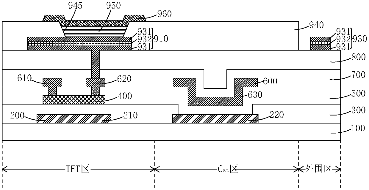
[0051] Step 1, such as Figure 4 As shown, a base substrate 10 is provided, a gate 20 is formed on the base substrate 10 , and a gate insulating layer 30 covering the gate 20 is formed on the base substrate 10 .

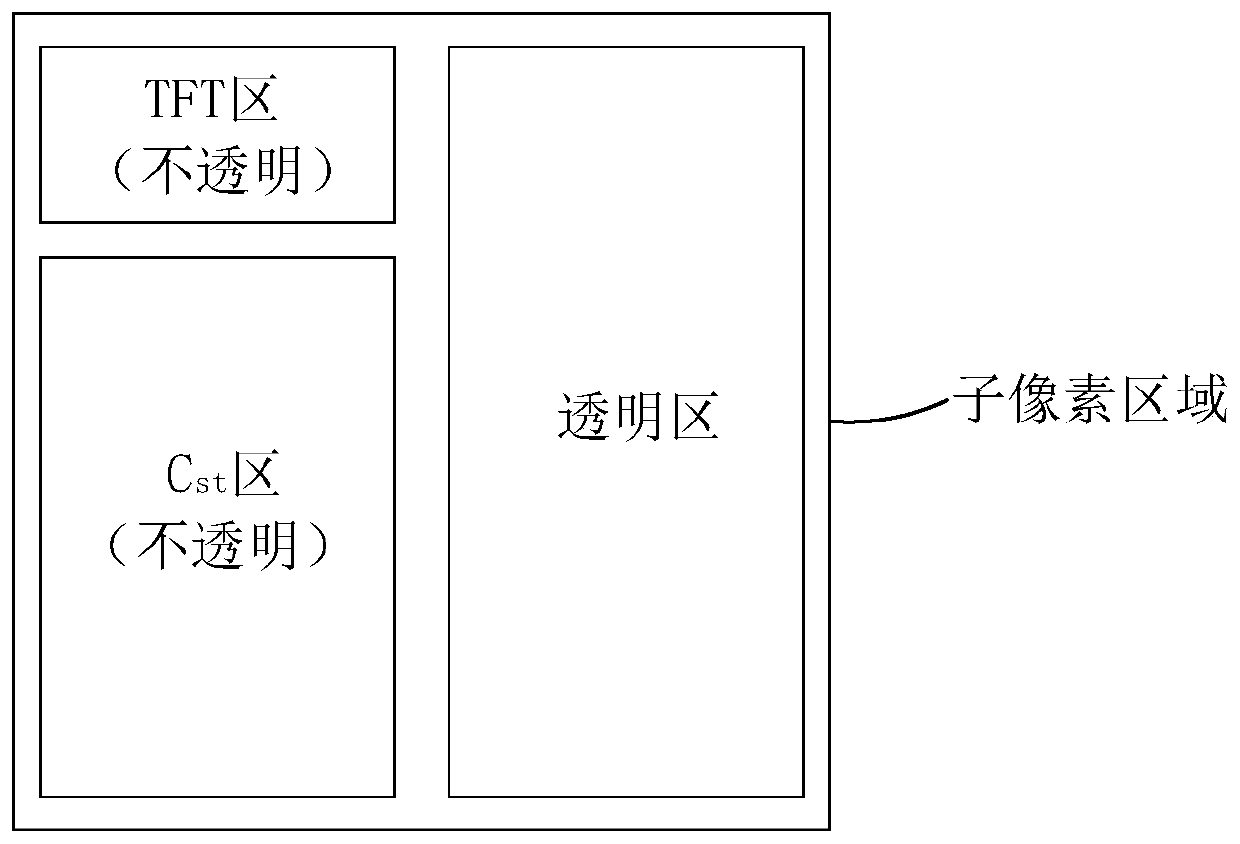
[0052] Specifically, the base substrate 10 includes a display area and a peripheral area located around the display area.

[0053] Specifically, the preparation method of the gate 20 includes: depositing a gate metal material on the base substrate 10 , and patterning the gate metal material by using a photolithography process to obtain the gate 20 .

[0054] Specifically, the gate 20 includes a first gate ...


PUM


Abstract

The invention provides a transparent OLED display and a manufacturing method thereof. In the manufacturing method of the transparent OLED display of the present invention, the active layer and the first storage capacitor electrode are formed in the same process, so that the first storage capacitor electrode is prepared from a transparent metal oxide semiconductor material, and the anode is fabricated through two photolithography processes and the second storage capacitor electrode, so that the second storage capacitor electrode is only made of transparent conductive oxide material, so that the storage capacitor region where the first storage capacitor electrode and the second storage capacitor electrode are located appears as a transparent area, improving the transparent OLED The light transmittance of the display improves the transparent display effect of the transparent OLED display. Further, while making the anode and the second storage capacitor electrode, form the connecting terminal located in the peripheral area, so that the connecting terminal is only made of transparent conductive oxide material, prevent it from being corroded by external water and oxygen, and improve the service life of the transparent OLED display .

Description

technical field [0001] The invention relates to the field of display technology, in particular to a transparent OLED display and a manufacturing method thereof. Background technique [0002] Organic light-emitting diode (Organic Light-Emitting Diode, OLED) display, also known as organic electroluminescent display, is a new type of flat panel display device, due to its simple preparation process, low cost, low power consumption, high luminance, Wide range of working temperature, light and thin size, fast response speed, easy to realize color display and large-screen display, easy to realize matching with integrated circuit driver, easy to realize flexible display, etc., so it has broad application prospects. [0003] With the development of display technology, a transparent display device has been proposed as a novel display method. This transparent display device can not only see the displayed image from the front of the screen, but also can see the objects on the back of th...

Claims


Application Information

Patent Timeline
Patent Type & Authority Patents(China)
IPC IPC(8): H01L27/32H01L49/02H01L21/77
CPCH01L28/60H10K59/131H10K59/1201
Inventor 刘兆松任章淳
Owner SHENZHEN CHINA STAR OPTOELECTRONICS SEMICON DISPLAY TECH CO LTD
Why Eureka
Try Eureka