Chip transferring device

A chip transfer and chip technology, applied in transportation and packaging, electrical components, semiconductor/solid-state device manufacturing, etc., can solve the problems of low transfer efficiency and high production costs, and achieve the effect of improving transfer efficiency and reducing transfer costs

Pending Publication Date: 2019-10-18
SHENZHEN SITAN TECH CO LTD
View PDF0 Cites 3 Cited by
  • Summary
  • Abstract
  • Description
  • Claims
  • Application Information

AI Technical Summary

Problems solved by technology

[0003] Transfer is a key technology in the field of Micro-LED chips. The traditional transfer method is generally: cutting a large number of Micro-LED chips on the ready-made chip board one by one, and then transfer them one by one (or dozens of them together) to the target part. , the transfer efficiency is low, the production cost is high, and it is not suitable for the preparation process of high-precision display screens

Method used


Image

  • Chip transferring device
  • Chip transferring device
  • Chip transferring device

Examples


Embodiment 1

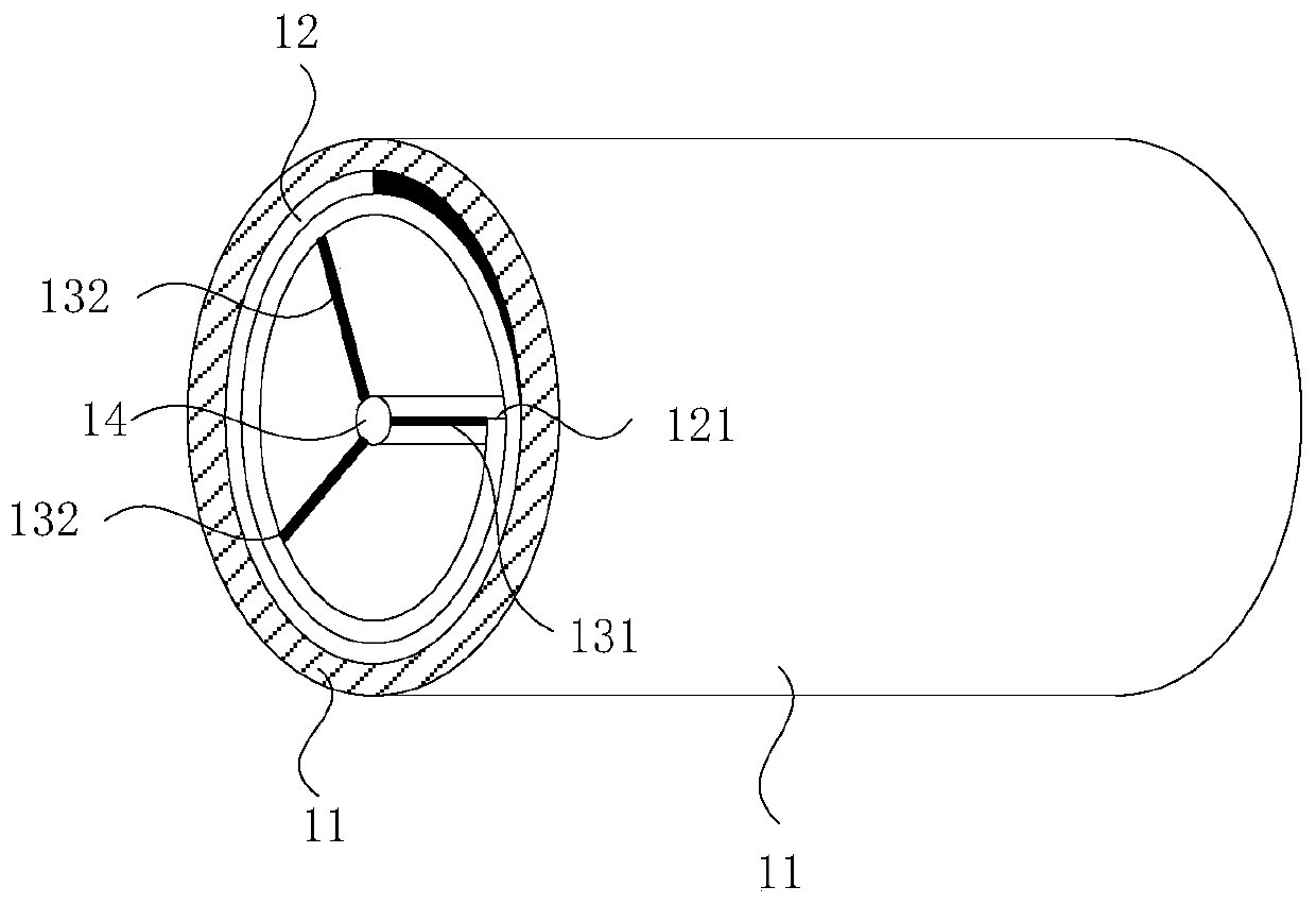
[0050] figure 1 It is a schematic diagram of the chip transfer device provided by Embodiment 1 of the present invention. The chip transfer device of this embodiment specifically includes: an elastic body 11 , a first rolling body 12 , a first support portion, and a first set of rods 14 .

[0051] The elastic body 11 is hollow and cylindrical, and is used for absorbing the cut chips. Specifically, the elastic body 11 is made of rubber and has a uniform hollow tubular shape with a certain expansion ability in the horizontal and vertical directions. The elastic layer also includes an adhesive layer on the outside, and the adhesive layer is used to absorb the cut chips.

[0052] The first rolling body 12 is hollow inside and is cylindrical, and is placed inside the elastic body 11 for supporting the cylindrical elastic body 11 and adjusting the radius of the elastic body 11. Specifically, the first rolling body 12 is made of The rigid material is curled to form a helix, and the a...

Embodiment 2

[0068] Figure 8 For the chip transfer device provided in this embodiment, compared with the chip transfer device in Embodiment 1, the chip transfer device in this embodiment further includes: at least one second rolling body, at least one second supporting part, at least one second set of rods .

[0069] At least one second rolling body 22 is hollow inside and is cylindrical, similar to the first rolling body 12 such as Figure 9 The nested sliding connection shown is used to support the cylindrical elastic body and adjust the length and radius of the elastic body 11 . Specifically, the second rolling body is coiled by a rigid material to form a spiral shape, and the appearance of the second rolling body is in the shape of a circular roll. Sliding and stretching between the first roll body 12 and the second roll body 22 can adjust the total length of the first roll body 12 and the second roll body 22 to adjust the length of the elastic body.

[0070] At least one second su...


PUM


Abstract

The invention discloses a chip transferring device. The chip transferring device comprises an elastic body, a first roll body, a first supporting part and a first sleeve rod; the elastic body is hollow inside and cylinder-shaped; the elastic body is used for adsorbing cut chips; the first roll body is hollow inside and is cylinder-shaped; the first roll body is arranged inside the elastic body andused for supporting the cylindrical elastic body and adjusting the radius of the elastic body; the first supporting part is arranged in the first roll body and used for supporting the first roll bodyand adjusting the radius of the first roll body; and the first sleeve rod is arranged in the first roll body and used for fixing the first supporting part. According to the technical schemes of the invention, the elastic body, the first roll body and the first supporting part are adopted; the radius of the elastic body used for adsorbing the chips is adjusted through the adjustable first supporting part, so that intervals between the chips can be adjusted; a large number of chips can be transferred; the transfer efficiency of the chips can be increased; the transfer cost of the chips can be decreased; and the density adjustment of the chips during chip transfer is realized.

Description

technical field [0001] The embodiment of the present invention relates to a chip transfer technology, in particular to a chip transfer device. Background technique [0002] Micro-LED is a new generation of display technology, which has higher brightness and better luminous efficiency than the existing OLED technology, but lower power consumption. Micro-LED has a series of advantages, and it is foreseeable that it will be widely used in the field of display technology in the future. [0003] Transfer is a key technology in the field of Micro-LED chips. The traditional transfer method is generally: cutting a large number of Micro-LED chips on the ready-made chip board one by one, and then transfer them one by one (or dozens of them together) to the target part. , the transfer efficiency is low, the production cost is high, and it is not suitable for the preparation process of high-precision display screens. Contents of the invention [0004] The invention provides a chip t...

Claims


Application Information

Patent Timeline
Patent Type & Authority Applications(China)
IPC IPC(8): H01L21/677H01L21/683
CPCH01L21/677H01L21/683
Inventor 刘召军邱成峰莫炜静郑汉宇
Owner SHENZHEN SITAN TECH CO LTD
Why Eureka
Try Eureka