Chemical palladium solution applied to chemical gold palladium gold plating on pcb
A chemical gold and coating technology, applied in liquid chemical plating, metal material coating process, coating, etc., can solve the problems that are difficult to deal with fine and complex electronic circuit design products, and achieve excellent ductility and stable coordination system , better bending resistance
- Summary
- Abstract
- Description
- Claims
- Application Information
AI Technical Summary
Problems solved by technology
Method used
Image
Examples
Embodiment 1
[0075] Palladium sulfate (as Pd 2+ total): 0.3g / L, ethylenediamine: 5g / L, 4-fluorobenzylamine: 2g / L, hydroxylamine sulfate: 3g / L, 7-(diethylamino)coumarin: 15mg / L, glycine: 5g / L, ammonium sulfate: 8g / L, tetrabutylammonium bisulfate: 2mg / L temperature: 60°C, pH7.5.
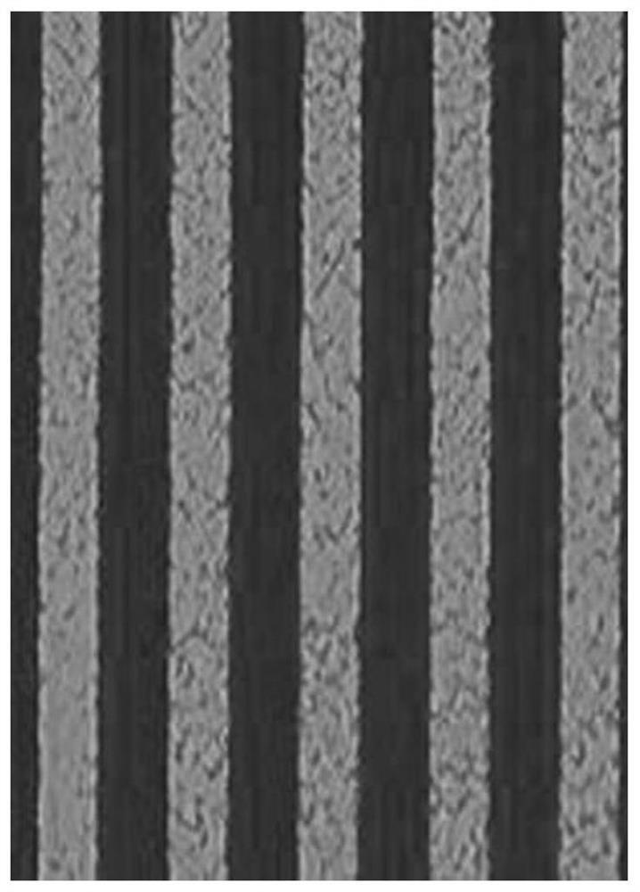
[0076] The appearance of the palladium layer obtained under the above parameters is flat and bright, there is no penetration plating on the fine lines, there is no missing plating in the micro and blind holes, and the lines are not whitish or falling off. The thickness of the coating is 4.3μinch (plating for 15 minutes). The stability of the solution reaches 6MTO (the circular experiment of palladium plating on the copper substrate is carried out. In the case of the plating solution with a palladium concentration of 0.3g / L in the construction of the tank, it is called 1MTO to deposit 0.3g / L palladium on the substrate), 3M Adhesive force of adhesive tape coating is good. At the same time, after the bending resista...
Embodiment 2
[0078] Palladium Ammonium Sulfate (as Pd 2+ Total): 0.6g / L, ethylenediamine: 10g / L, benzylamine: 1g / L, N,N-diethylhydroxylamine: 10g / L, 7-(diethylamino)coumarin: 50mg / L , Glycine: 1g / L, Ammonium Sulfate: 4g / L, Tetrabutylammonium Bisulfate: 0.1mg / L Temperature: 40°C, pH 7.0
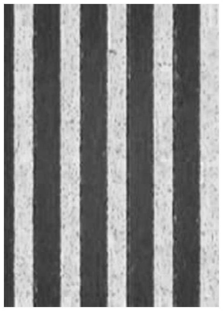
[0079] The appearance of the palladium layer obtained under the above parameters is flat and bright, there is no penetration plating on the fine lines, there is no missing plating in the micro and blind holes, and the lines are not whitish or falling off. The thickness of the coating is 3.2μinch (plating for 10 minutes). Liquid stability up to 6MTO, 3M adhesive tape coating has good adhesion. At the same time, after the bending resistance test of the coating, no obvious cracks were observed at 100 times magnification; the solder test showed that the pads were well wetted and the tin was full; the bonding performance was excellent, and the gold wire tensile test reached more than 10g.
Embodiment 3
[0081] Palladium Ammonium Sulfate (as Pd 2+ Total): 0.4g / L, furfurylamine: 5g / L, benzylamine: 10g / L, D-mannitol: 2g / L, thiodiglycolic acid: 100mg / L, glycine: 3g / L, ammonium sulfate : 15g / L, cetyltrimethylammonium bisulfate: 5mg / L Temperature: 50℃, pH 7.2
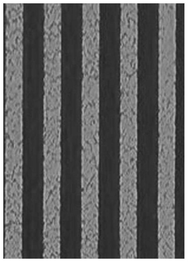
[0082] The appearance of the palladium layer obtained under the above parameters is smooth and bright, there is no penetration plating on the fine lines, there is no missing plating in the micro and blind holes, and the lines are not whitish or falling off. The thickness of the coating is 4.6μinch (plating for 15 minutes). Liquid stability reaches 5.5MTO, 3M adhesive tape coating has good adhesion. At the same time, after the bending resistance of the coating, no obvious cracks were observed when magnified 100 times; the solder test showed that the pads were well wetted and the tin was full; the bonding performance was excellent, and the gold wire tensile test reached more than 10g.
PUM
 Abstract
Description
Claims
Application Information
 - R&D
- Intellectual Property
- Life Sciences
- Materials
- Tech Scout
- Unparalleled Data Quality
- Higher Quality Content
- 60% Fewer Hallucinations
Browse by: Latest US Patents, China's latest patents, Technical Efficacy Thesaurus, Application Domain, Technology Topic, Popular Technical Reports.
© 2025 PatSnap. All rights reserved.Legal|Privacy policy|Modern Slavery Act Transparency Statement|Sitemap|About US| Contact US: help@patsnap.com


