Copper foil resistor and circuit board structure having the same
A technology of circuit boards and copper foils, applied in circuits, resistors, printed circuits, etc., can solve problems such as joint improvement, peeling, copper foil resistance 17 plating density and continuity are not perfect, etc.
- Summary
- Abstract
- Description
- Claims
- Application Information
AI Technical Summary
Problems solved by technology
Method used
Image
Examples
Embodiment 1
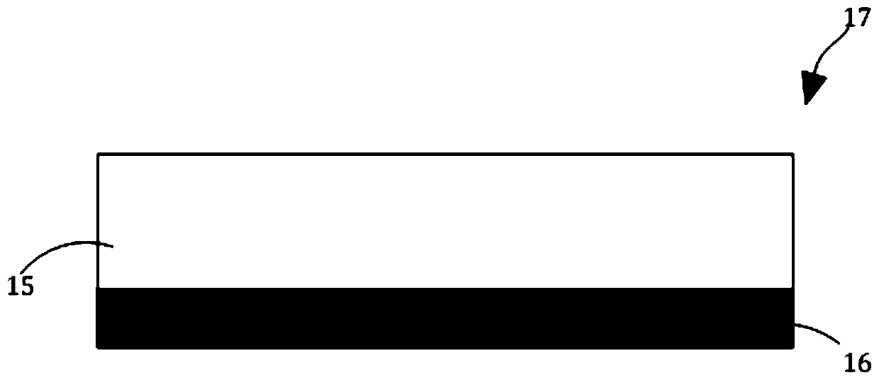
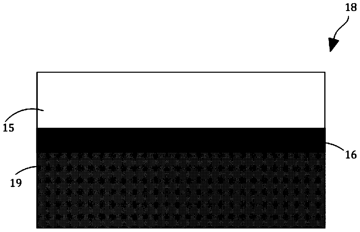
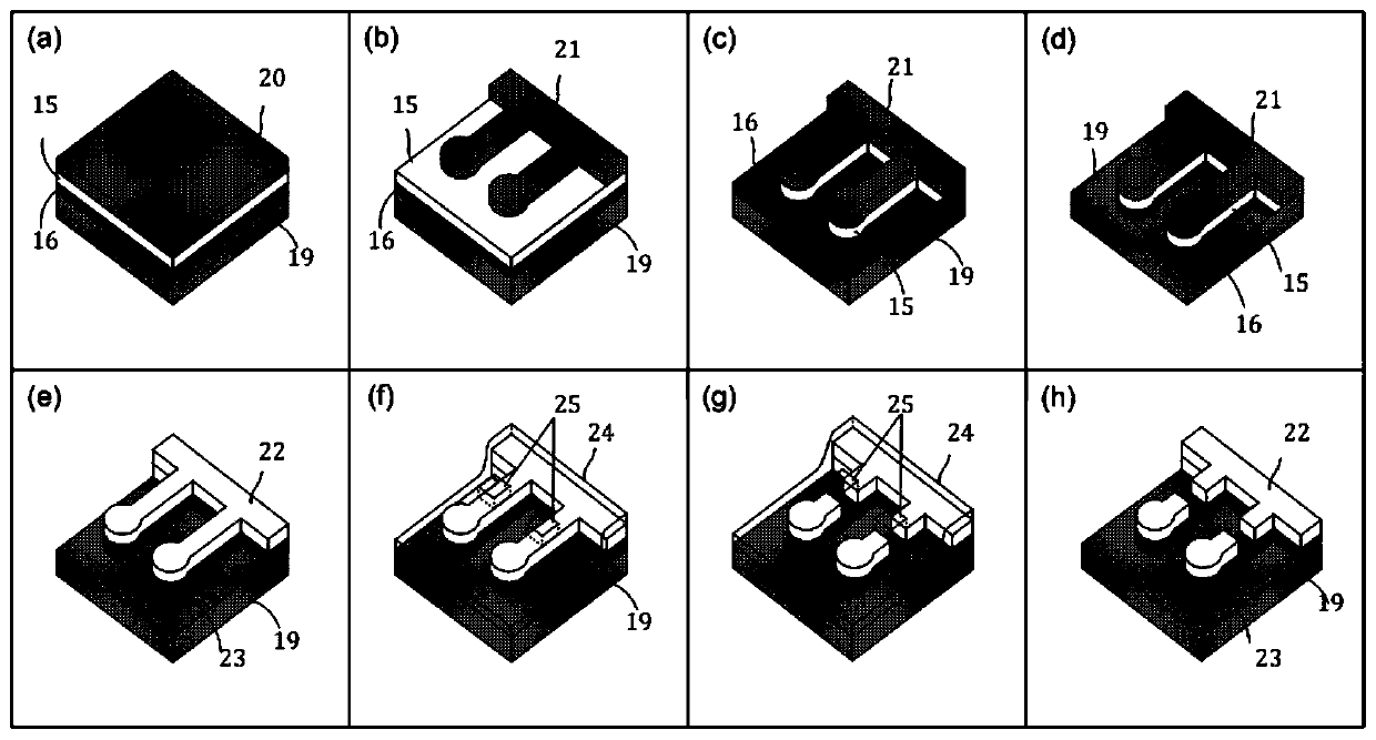
[0053] Figure 4 A perspective view showing a copper foil resistor of the present invention. The copper foil resistor 1 of the present invention is suitable for being combined with a substrate 10 to form a circuit board structure 2, and the substrate 10 can be a flexible substrate (eg PET) or a rigid substrate (eg glass fiber board). Figure 5 That is, it shows the first perspective view of the structure of the circuit board including the copper foil resistor of the present invention. In particular, after performing at least one developing and etching process on the circuit board structure 2 including the copper foil resistor 1 of the present invention, an electronic circuit including at least one thin film resistor component can be fabricated on the circuit board structure 2 . According to the design of the present invention, the copper foil resistor 1 includes a first conductive metal layer 11 and a first resistance layer 12 ; wherein, the thickness of the first conductive ...
Embodiment 2
[0062] Figure 7 A second perspective view showing a circuit board structure comprising the copper foil resistor of the present invention. Compare Figure 5 and Figure 7 It can be found that a second conductive metal layer 13 can be further connected to the other surface of the substrate 10 to obtain a double-sided circuit board structure with single-sided copper foil and single-sided copper foil resistor 1 .
Embodiment 3
[0064] Figure 8 A third perspective view showing a circuit board structure comprising a copper foil resistor of the present invention. Compare Figure 5 and Figure 8It can be found that another copper foil resistor 9 can be further connected to the other surface of the substrate 10 to obtain a double-sided circuit board structure with copper foil resistors on both sides. The copper foil resistor 9 includes: a second conductive metal layer 13 and a second resistive layer 14; wherein, the second resistive layer 14 is formed on the second conductive metal layer 13, and is also made of chromium, tungsten, nickel metal compound, Chromium metal compounds, tungsten metal compounds, nickel-based alloys, chromium-based alloys or tungsten-based alloys. Moreover, the copper foil resistor 9 is connected to the other surface of the substrate 10 with its second resistor layer 14 .
PUM
| Property | Measurement | Unit |
|---|---|---|
| thickness | aaaaa | aaaaa |
| thickness | aaaaa | aaaaa |
| thickness | aaaaa | aaaaa |
Abstract
Description
Claims
Application Information
 - R&D Engineer
- R&D Manager
- IP Professional
- Industry Leading Data Capabilities
- Powerful AI technology
- Patent DNA Extraction
Browse by: Latest US Patents, China's latest patents, Technical Efficacy Thesaurus, Application Domain, Technology Topic, Popular Technical Reports.
© 2024 PatSnap. All rights reserved.Legal|Privacy policy|Modern Slavery Act Transparency Statement|Sitemap|About US| Contact US: help@patsnap.com


