An active high-density electrode array and its preparation method
An electrode array and active electrode technology, applied in the field of electrode arrays, can solve problems such as noise, and achieve the effects of improving signal quality, improving noise, light, thin, transparent and flexible power consumption
- Summary
- Abstract
- Description
- Claims
- Application Information
AI Technical Summary
Problems solved by technology
Method used
Image
Examples
Embodiment 1
[0038] The active high-density electrode array provided in this embodiment adopts a matrix vertical and horizontal arrangement, and 64 active amplifying circuits and 64 electrodes are arranged as follows: figure 1 structure shown. In the later stage, different spatial filtering methods are realized through subsequent processing software, such as the common vertical single / double difference, horizontal single / double difference, double difference, etc. At the same time, the active high-density electrode array provided in this embodiment adopts an 8*8 electrode array, which provides favorable assistance for analyzing surface electromyographic signals of muscles of different complexity due to the increase of acquisition channels. Among them, the circular patterns arranged in 8*8 are electrodes for collecting electromyographic signals.
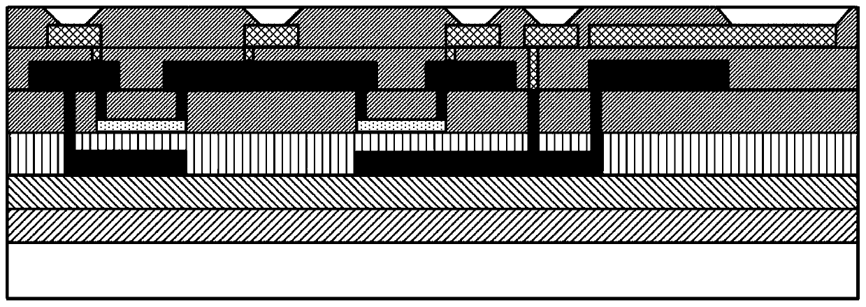
[0039] Such as figure 2 As shown, the active electrode unit provided in this embodiment is formed by integrating electrodes and active amplifie...
Embodiment 2
[0049] The preparation method of the active high-density electrode array provided in this embodiment includes the following steps:
[0050] The first step is the preparation of the flexible active electrode substrate.
[0051] Such as Figure 4 The schematic diagram of the structure of the flexible polyimide film substrate is shown, and the process steps are roughly as follows: spin-coat PI reagent on the cleaned glass substrate 1, and set the rotation speed to 500RPM (30s). After that, the following annealing steps are carried out: 80°C (30min)——100°C (60min)——200°C (60min)——300°C (30min)——400°C (10min) for annealing treatment, and then naturally cool down to room temperature. In order to ensure the adhesion of other films on the polyimide film layer 2, a buffer layer 3 composed of 300nm SiNx and 200nm SiO2 is prepared by plasma enhanced chemical vapor deposition. So far, the preparation of a flat and transparent flexible polyimide film substrate is completed.
[0052] The...
PUM
| Property | Measurement | Unit |
|---|---|---|
| diameter | aaaaa | aaaaa |
| thickness | aaaaa | aaaaa |
Abstract
Description
Claims
Application Information
 - R&D
- Intellectual Property
- Life Sciences
- Materials
- Tech Scout
- Unparalleled Data Quality
- Higher Quality Content
- 60% Fewer Hallucinations
Browse by: Latest US Patents, China's latest patents, Technical Efficacy Thesaurus, Application Domain, Technology Topic, Popular Technical Reports.
© 2025 PatSnap. All rights reserved.Legal|Privacy policy|Modern Slavery Act Transparency Statement|Sitemap|About US| Contact US: help@patsnap.com


