
VCSEL chip with high recombination efficiency and manufacturing method thereof

A technology of recombination efficiency and manufacturing method, which is applied to the structure of the active area, laser parts, electrical components, etc., and can solve the problems of low stimulated emission rate and low recombination efficiency of quantum well design.

Pending Publication Date: 2019-09-03
威科赛乐微电子股份有限公司
View PDF3 Cites 3 Cited by
  • Summary
  • Abstract
  • Description
  • Claims
  • Application Information

AI Technical Summary

Problems solved by technology

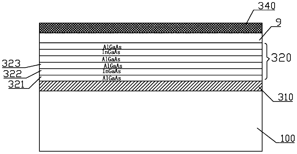
However, most of the quantum wells in VCSEL chips in the prior art are matched with InGaAs / GaAs as potential wells and potential barriers respectively, and the allocation of MQW recombination efficiency that determines the same level of quantity is basically only affected by GaAs potential barriers, so the prior art The recombination efficiency of the quantum well design is low, and the stimulated emission rate has not been high

Method used


Image

  • VCSEL chip with high recombination efficiency and manufacturing method thereof
  • VCSEL chip with high recombination efficiency and manufacturing method thereof
  • VCSEL chip with high recombination efficiency and manufacturing method thereof

Examples


Embodiment Construction

[0027] In order to make the object, technical solution and advantages of the present invention clearer, the present invention will be further described in detail below in conjunction with specific embodiments and with reference to the accompanying drawings.

[0028]It should be noted that in the drawings or descriptions, similar or identical parts use the same figure numbers, and implementations not shown or described in the drawings are forms known to those of ordinary skill in the art. Additionally, while illustrations of parameters including particular values ​​may be provided herein, it should be understood that the parameters need not be exactly equal to the corresponding values, but rather may approximate the corresponding values ​​within acceptable error margins or design constraints. The directional terms mentioned in the embodiments, such as "up", "down", "top", "bottom", "left", "right", etc., are only referring to the directions of the drawings, and are not intended ...


PUM

PropertyMeasurementUnit
Thicknessaaaaaaaaaa

Abstract

The invention relates to the technical field of laser chips, in particular to a VCSEL chip with high recombination efficiency and a manufacturing method thereof. The VCSEL chip comprises a substrate,an epitaxial layer and an N-contact, the epitaxial layer comprises an N-DBR, a quantum well, an oxide layer and a P-DBR, the P-DBR, the oxide layer and the quantum well are etched to the surface of the N-DBR to form a table top, the quantum well comprises a plurality of pairs of quantum well composite layers, each quantum well composite layer comprises AlxGaAs potential barriers, InGaAs potentialwells and AlxGaAs potential barriers which are grown in an overlapping mode, the P-DBR is divided into a central area, a middle area and an edge area, the central area is a light outlet hole, a firstSiNx layer grows on the P-DBR at the position corresponding to the central area, a P-contact is evaporated on the P-DBR at the position corresponding to the middle area, and a second SiNx layer growson the P-DBR at the position corresponding to the edge area. The potential barrier in the quantum well in the VCSEL chip has high forbidden bandwidth, lattice matching is easy to achieve, more electrons are intensively bound in the quantum well, excitation probability is increased, composite efficiency is improved, and therefore, stimulated radiation with higher efficiency is achieved.

Description

technical field [0001] The invention relates to the technical field of laser chips, in particular to a VCSEL chip with high recombination efficiency and a manufacturing method thereof. Background technique [0002] Vertical cavity surface emitting laser (Vertical Cavity Surface Emitting Laser) chip, also known as VCSEL chip or vertical cavity surface emitting laser chip, is a laser emitting chip based on gallium arsenide semiconductor material, and its laser is emitted perpendicular to the top surface. Unlike the general independent chip process of dicing, the edge-fired laser is different from the edge-fired laser. VCSEL chips have the advantages of small size, circular output spot, single longitudinal mode output, low threshold current, low price, and easy integration into large-area arrays. They are widely used in optical communication, optical interconnection, optical storage and other fields. [0003] A laser resonator is composed of two distributed Bragg reflectors (D...

Claims


Application Information

Patent Timeline
IPC IPC(8): H01S5/183H01S5/187H01S5/34H01S5/343
CPCH01S5/183H01S5/18361H01S5/187H01S5/34H01S5/3432
Inventor 窦志珍曹广亮刘留苏小平
Owner 威科赛乐微电子股份有限公司
Learn More