
A method and device for measuring energy band bending by photoelectron spectroscopy

A photoelectron energy spectrum and energy band bending technology, which is applied in the direction of measuring devices, material analysis using wave/particle radiation, instruments, etc., can solve the problem of inaccurate measurement of energy band bending

Active Publication Date: 2022-03-08
SUZHOU INST OF NANO TECH & NANO BIONICS CHINESE ACEDEMY OF SCI
View PDF7 Cites 0 Cited by
  • Summary
  • Abstract
  • Description
  • Claims
  • Application Information

AI Technical Summary

Problems solved by technology

When the sample to be tested has energy band bending, the energy level position calculated from the peak position information will move due to different integration ranges, resulting in inaccurate measurement of the energy band bending

Method used


Image

  • A method and device for measuring energy band bending by photoelectron spectroscopy
  • A method and device for measuring energy band bending by photoelectron spectroscopy
  • A method and device for measuring energy band bending by photoelectron spectroscopy

Examples


Embodiment Construction

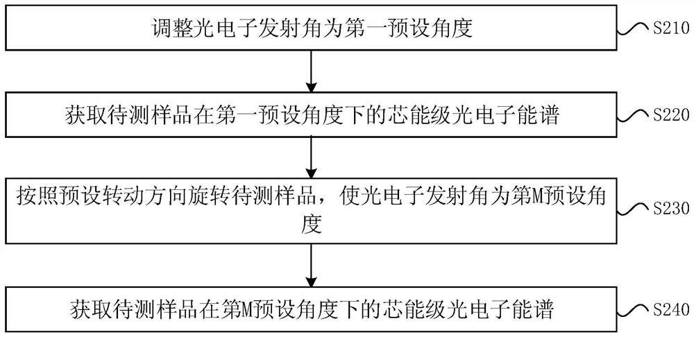
[0059] The present invention will be further described in detail below in conjunction with the accompanying drawings and embodiments. It should be understood that the specific embodiments described here are only used to explain the present invention, but not to limit the present invention. In addition, it should be noted that, for the convenience of description, only some structures related to the present invention are shown in the drawings but not all structures.

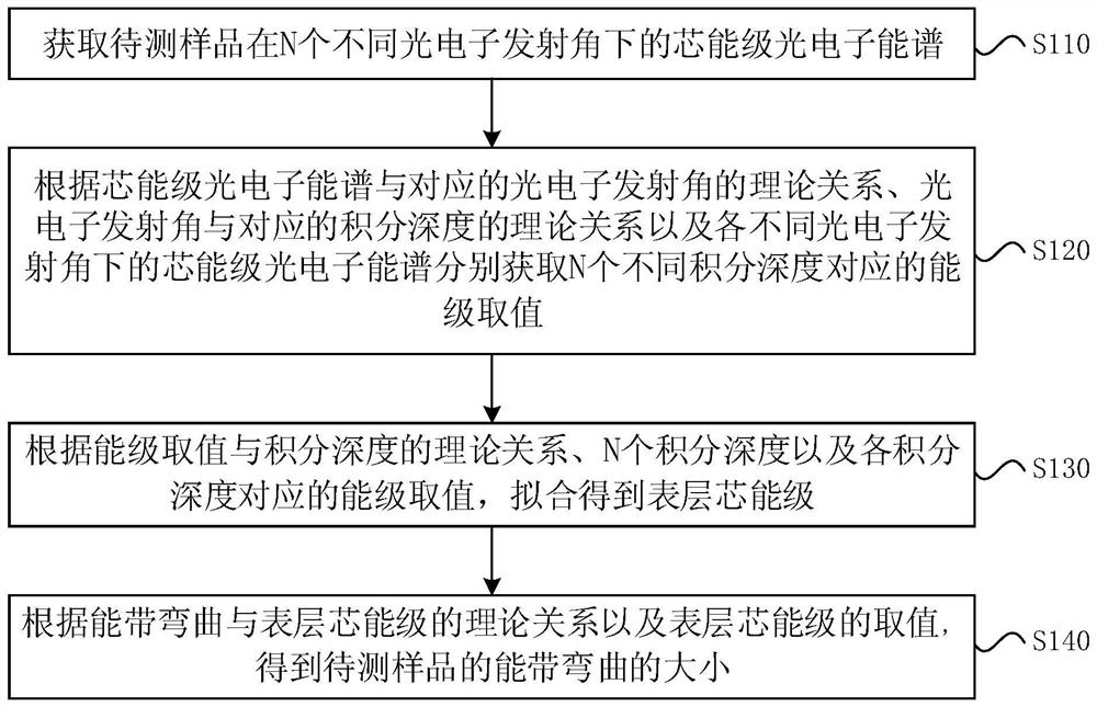
[0060] figure 1 It is a schematic flowchart of a method for measuring energy band bending by photoelectron spectroscopy provided by an embodiment of the present invention. refer to figure 1 , the method for measuring band bending includes:

[0061] S110. Obtain core-level photoelectron spectra of the sample to be tested under N different photoelectron emission angles.

[0062] Wherein, N is an integer and N≥4. In the subsequent steps, since it is necessary to obtain theoretical data by fitting the measured dat...


PUM


Abstract

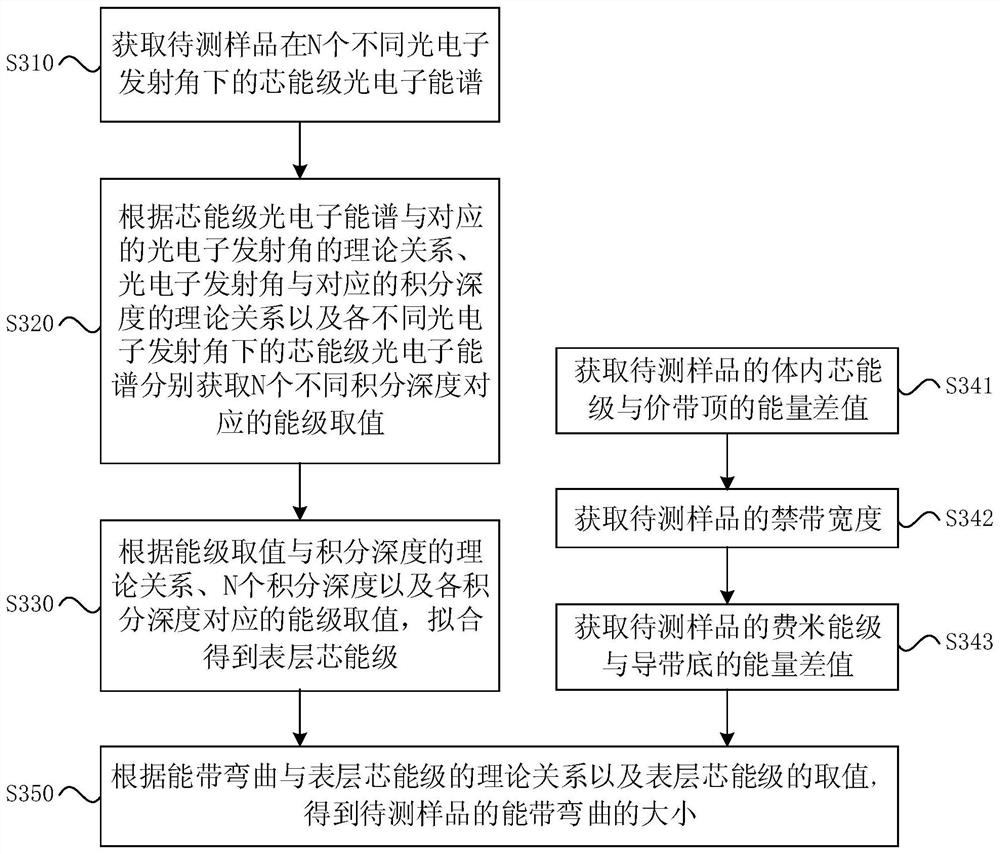
The invention discloses a method and a device for measuring energy band bending by photoelectron energy spectrum. The method includes: obtaining the core level photoelectron spectrum of the sample to be tested under N different photoelectron emission angles; N is an integer and N≥4; according to the theoretical relationship between the core level photoelectron spectrum and the corresponding photoelectron emission angle, the photoelectron The theoretical relationship between the emission angle and the corresponding integration depth and the core level photoelectron spectrum under different photoelectron emission angles respectively obtain the energy level values ​​corresponding to N different integration depths; the photoelectron emission angle corresponds to the integration depth one by one; according to the energy The theoretical relationship between the level value and the integration depth, the N integration depths and the energy level values ​​corresponding to each integration depth are fitted to obtain the surface core energy level; the surface core energy level is the corresponding core energy level when the integration depth is 0; according to The theoretical relationship between the energy band bending and the surface core energy level and the value of the surface core energy level can be used to obtain the size of the energy band bending of the sample to be tested. Thereby, the measurement accuracy of band bending can be improved.

Description

technical field [0001] Embodiments of the present invention relate to the technical field of semiconductor property measurement, and in particular to a method and device for measuring band bending using photoelectron spectroscopy. Background technique [0002] Band bending may refer to an equilibrium state in which potential energy is balanced by electron flow after two materials with different work functions and energy band structures are in contact, corresponding to a flat-band state. Two different semiconductor contacts, semiconductor and metal contact and semiconductor and electrolyte contact, etc. will form energy band bending. Band bending has a crucial impact on the performance of semiconductor devices. [0003] At present, there are mainly three kinds of equipment for measuring energy band bending, namely ultraviolet photoelectron spectroscopy, surface electrostatic potential atomic force microscope and X-ray photoelectron spectroscopy with fixed photoelectron emiss...

Claims


Application Information

Patent Timeline
Patent Type & Authority Patents(China)
IPC IPC(8): G01N23/2273
CPCG01N23/2273G01N2223/085G01N2223/321
Inventor 赵弇斐丁孙安
Owner SUZHOU INST OF NANO TECH & NANO BIONICS CHINESE ACEDEMY OF SCI
Learn More