Method for predicting doping modification performance of rare earth
A prediction method and performance prediction technology, applied in the fields of materials and physics, can solve problems such as poor detection performance, and achieve the effects of economic convenience, solving detection modification performance, and simple operation.
- Summary
- Abstract
- Description
- Claims
- Application Information
AI Technical Summary
Problems solved by technology
Method used
Image


Examples
Embodiment 1
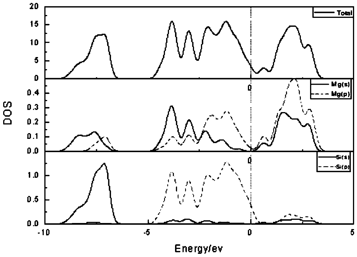
[0074] see Figure 3-Figure 6 , respectively Mg 2 Si, Mg 7 Si 4 La, Mg 8 Si 4 La and Mg 8 Si 3 Schematic diagram of the total density of states and the partial density of states of La.
[0075] Figure 2-5 The abscissa represents the energy, and the ordinate represents the density of states.
[0076] The valence electrons of each element are: Mg2p 6 3s 2 , Si3s 2 p 2 , La5s 2 5p 6 5d 1 , the dotted line is the Fermi level, which corresponds to zero energy.
[0077] Mg 2 The bonding electrons of Si and its solid solutions are mainly concentrated in the range of -5 to 3 eV, and the intrinsic Mg 2 The bonding electrons of Si are mainly contributed by Si(3p), Mg(2p) and Mg(3s).
[0078] After the La atom is doped, the bonding electrons La(5s) and La(5p) enter the conduction band, and the interaction with Si(3s) and Si(3p) makes the doped solid solution have metallic conductivity.
Embodiment 2
[0080] see Figure 7-Figure 10 , respectively Mg 2 Si, Mg 7 Si 4 La, Mg 8 Si 3 La and Mg 8 Si 4 Schematic diagram of the energy band diagram of La.
[0081] Figure 6-Figure 9 The middle abscissa represents K-space, and the ordinate represents energy. The dotted line in the figure represents the Fermi surface, above the Fermi surface is the conduction band, the bottom of the conduction band is the lowest energy level of the conduction band, below the Fermi line is the valence band, and the bottom of the valence band is the fullest energy level of the valence band.
[0082] Intrinsic Mg 2 The Fermi level of Si does not intersect multiple energy bands, and the Fermi level is between the bottom of the conduction band and the top of the valence band, indicating that Mg 2 Si has semiconductor properties, the lowest point of the conduction band and the highest point of the valence band have the same K value, Mg 2 The energy gap of Si is a direct energy gap.
[0083] When...
Embodiment 3
[0086] see Figure 11-Figure 14 , respectively Mg 2 Si, Mg 7 Si 4 La, Mg 8 Si 3 La and Mg 8 Si 4 Schematic diagram of the differential charge density map of the (110) plane of La.
[0087] Contours are drawn from -0.04137eV / atom 3 Draws to 0.03488eV / atom 3 .
[0088] in Mg 2 In Si, Mg-Mg has no obvious directional bond, and Mg-Mg is a metallic bond; the charge distribution between Si-Si shows that the bonding ability between Si-Si is strong and covalent bond. The charge distribution between Mg-Si is obviously deformed, and a large number of charges tend to Si atoms, forming strong ionic bonds. After doping with La atoms, the charge transfer phenomenon occurs between La and Mg and Si atoms, forming La-Mg ionic bonds and La-Si ionic bonds.
[0089] The newly generated La-Si and La-Mg ionic bonds increase the structural stability, which is mainly determined by the elastic properties.
[0090] The electrical properties are mainly based on the density of states and the...
PUM
 Abstract
Description
Claims
Application Information
 - R&D
- Intellectual Property
- Life Sciences
- Materials
- Tech Scout
- Unparalleled Data Quality
- Higher Quality Content
- 60% Fewer Hallucinations
Browse by: Latest US Patents, China's latest patents, Technical Efficacy Thesaurus, Application Domain, Technology Topic, Popular Technical Reports.
© 2025 PatSnap. All rights reserved.Legal|Privacy policy|Modern Slavery Act Transparency Statement|Sitemap|About US| Contact US: help@patsnap.com